
Method of forming buried wiring lines, and substrate and display device using the same

Inactive Publication Date: 2008-10-02
NEC LCD TECH CORP
View PDF7 Cites 15 Cited by
  • Summary
  • Abstract
  • Description
  • Claims
  • Application Information

AI Technical Summary

Benefits of technology

[0030]An object of the present invention is to provide a method of forming buried wiring lines that makes it possible not to limit usable materials for an insulative plate to those having excellent heat resistance and to improve the corrosion resistance of the terminals provided for the buried wiring lines, and a substrate for a display device, and a display device.
[0049]In a preferred embodiment of the method of forming buried wiring lines according to the first aspect of the invention, between the step of selectively etching the surface of the insulative plate to form the grooves and the step of placing the metallic nanoparticle ink on the whole surface of the insulative plate to fill the grooves with the metallic nanoparticle ink, a step of giving ink-receptivity to the grooves is carried out to increase a surf ace energy of inner surf aces of the grooves. In this embodiment, there is an additional advantage that ink-receptivity is given to the inside surf aces of the grooves and therefore, the filling of the grooves with the metallic nanoparticle ink is surely carried out without voids even if the grooves are minute.

Problems solved by technology

As a result, the display quality will deteriorate due to the delay of the signals flowing through the wiring lines.
This leads to display quality degradation due to signal transmission delay also.
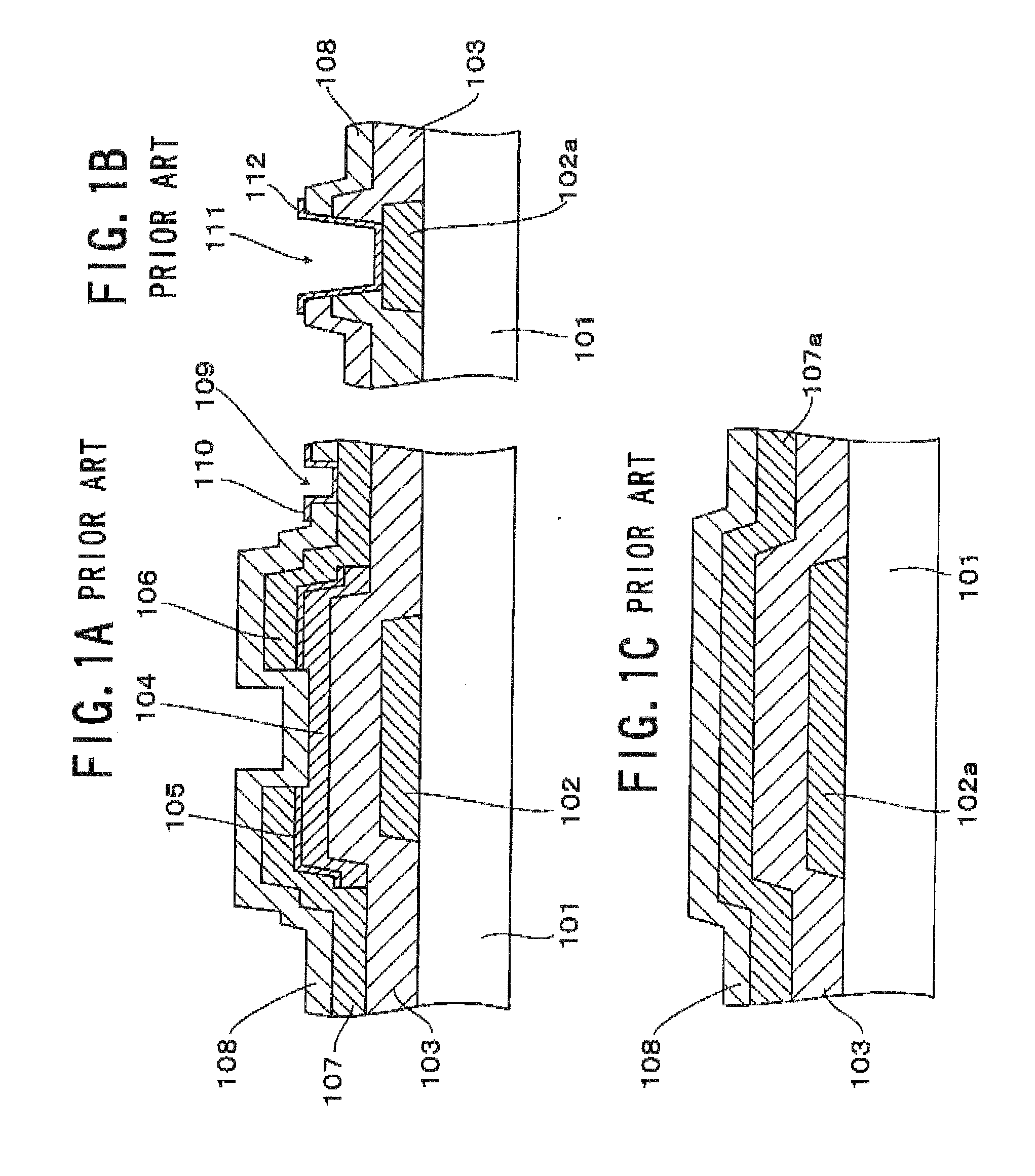
Therefore, defects or failures such as disconnection of the other wiring lines formed above the gate lines 102a and / or disclination due to the alignment distortion of the liquid crystal molecules are more likely to occur.
Accordingly, there is a problem that not only the reduction of the count of necessary processes is difficult, but also the equalization of the electric current density distribution in the plating solution (which is important for the plating reaction) is difficult if this method is applied to the insulative plate having a wide area or size.
Moreover, another problem that a huge amount of liquid waste needs to be processed occurs.
With the method of forming a metal film for gate electrodes and gate lines by a vacuum film formation method such as sputtering disclosed by the Patent Document 2, it is difficult to form the metal film uniformly in the depressions of the insulative plate.
In particular, since the step coverage of sputtering is poor, the thickness of the said metal film is likely to be relatively larger at the top ends of the depressions if the width of the depressions is small.
This means that it is difficult for the said metal film to have a uniform thickness oven in the deep inside of the depressions.
Accordingly, there is a problem that voids are likely to occur in the depressions and / or in the gate lines buried in the depressions, thereby degrading the chemical resistance and / or the corrosion resistance of the gate lines.
As a result, with the method of the Patent Document 2, there is another problem that the level difference to be formed on or over the gate electrodes and the gate lines is likely to be larger by the height corresponding to the thickness of the remaining part of the said metal film outside the depressions.
Therefore, there is a problem that usable insulative plates are limited to those having excellent heat resistance, in other words, usable materials for the insulative plate are limited.
Moreover, since an ordinary liquid organic metal contains metallic atoms as organic compounds, the content of the metallic ingredient is low.
This means that the volume shrinkage ratio after sintering due to the agglomeration is large.
For this reason, even if a person seeks to form metallic wiring lines having a desired thickness in the grooves by the method of the Patent Document 3, another problem that the thickness of the metallic wiring lines varies widely due to the large volume shrinkage ratio will occur.
Accordingly, with the method of the Patent Document 3, a further problem that the corrosion of the gate input terminals is likely to be triggered by the above-described impurities during the use of the LCD device will occur.
Therefore, if the interval between the wiring patterns is as large as several tens or several hundreds of micrometers (μm) similar to the wiring patterns used in the LCD device, the minute particle conductive paste may be unintentionally left between the wiring patterns.
As a result, there is a possibility that the metallic wiring lines formed in the grooves do not have a desired pattern.

Method used


Image

  • Method of forming buried wiring lines, and substrate and display device using the same
  • Method of forming buried wiring lines, and substrate and display device using the same
  • Method of forming buried wiring lines, and substrate and display device using the same

Examples


Embodiment Construction

[0085]Preferred embodiments of the present invention will be described in detail below while referring to the drawings attached.

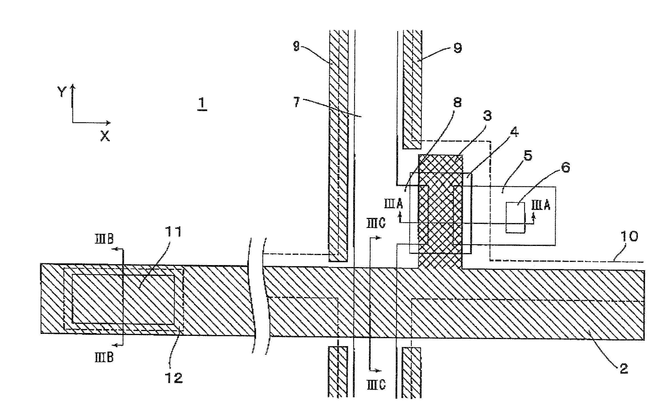
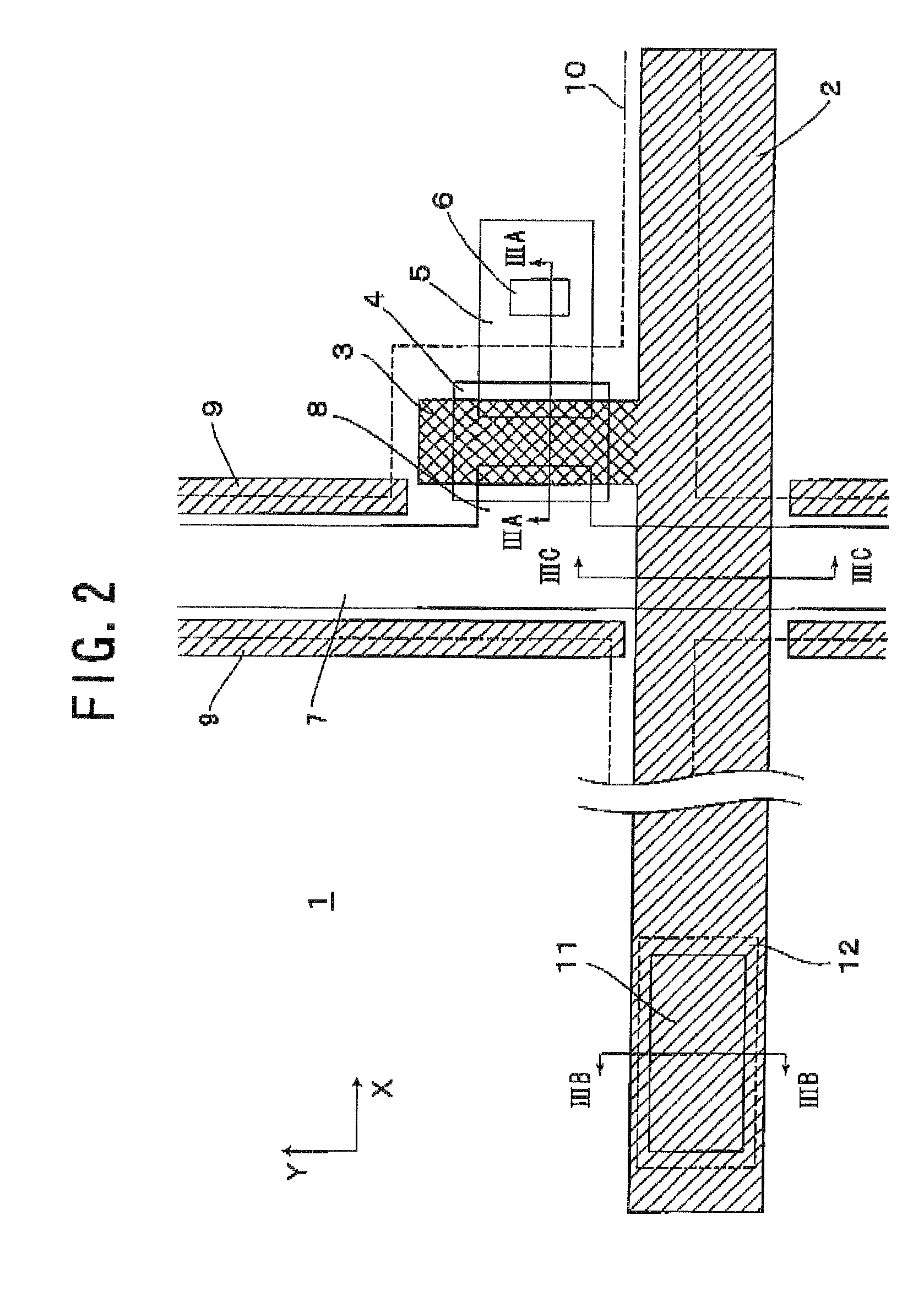
[0086]A TFT substrate of a LCD device to which a method of forming buried wiring lines according to an embodiment of the present invention is explained below with reference to FIG. 2 and FIGS. 3A to 3C. These figures show the structures of the TFT section, the gate input terminal section, and the intersecting section of the gate lines and the drain lines, respectively, which correspond to one of the pixels arranged in a matrix array on the TFT substrate, respectively.

[0087]As an insulative plate 1, a glass plate is used here. However, any other insulative plate than glass may be used. On the surface of the insulative plate 1, stripe-shaped gate lines 2 extending linearly along the row direction of the matrix (i.e., the X direction in FIG. 2), and gate electrodes 3 connected to the respective gate lines 2 are formed. The gate lines 2 and the gate electrodes ...


PUM

PropertyMeasurementUnit
Diameteraaaaaaaaaa
Diameteraaaaaaaaaa
Surface tensionaaaaaaaaaa

Abstract

An method of forming buried wiring lines makes it possible not to limit usable materials for an insulative plate to those having excellent heat resistance and to improve the corrosion resistance of the terminals provided for the buried wiring lines. The surface of an insulative plate is selectively etched using a mask formed on the surface, thereby forming grooves in the surface. A metallic nanoparticle ink is placed over the whole surface of the plate to fill the grooves with the ink, where the mask is being left. The ink is heated for preliminary curing to form a metallic nanoparticle ink film. The part of the film placed on the mask is selectively removed by detaching the mask, thereby leaving the remainder of the film in the grooves. The remaining film in the grooves is heated for main curing, thereby forming desired buried wiring lines.

Description

BACKGROUND OF THE INVENTION[0001]1. Field of the Invention[0002]The present invention relates to a method of forming buried wiring lines, a substrate for a display device including the buried wiring lines, and a display device including the substrate. More particularly, the present invention relates to a method of forming wiring lines buried in grooves formed in the surface of an insulative plate (i.e., buried wiring lines), a substrate for a display device using the method or the buried wiring lines thus formed, and a display device using the said substrate. The present invention is preferably applied to large area, high definition, and high aperture-ratio of Liquid-Crystal Display (LCD) devices using Thin-Film Transistors (TFTs).[0003]2. Description of the Related Art[0004]In recent years, the LCD device has been extensively used as a high-resolution display device. The LCD device comprises a substrate on which switching elements such as Thin-Film Transistors (TFTs) are formed (wh...

Claims


Application Information

Patent Timeline
IPC IPC(8): H05K3/40H05K1/11
CPCB82Y20/00G02F1/136286G02F2001/136295G02F2202/36H05K3/002H05K3/048Y10T29/49155H05K3/1258H05K2201/0257H05K2201/09036H05K2203/0571H05K2203/1131H05K3/107G02F1/136295
Inventor YASUDA, KYOUNEI
Owner NEC LCD TECH CORP
Learn More