Conductive ink composition and method of forming a conductive pattern using the same

a technology of conductive ink and composition, which is applied in the direction of inks, metal/alloy conductors, and conductors, etc., can solve the problems of environmental pollution, limited types of substrates used in optical patterning methods, and increased manufacturing costs so as to improve oxidation stability of conductive patterns, the effect of reducing the manufacturing cost of forming conductive patterns

Inactive Publication Date: 2008-10-02
SAMSUNG DISPLAY CO LTD
View PDF7 Cites 43 Cited by
  • Summary
  • Abstract
  • Description
  • Claims
  • Application Information

AI Technical Summary

Benefits of technology

[0010]The present invention provides a conductive ink composition capable of reducing manufacturing costs of a conductive pattern and improving the oxidation stability of a conductive pattern and a method of forming a conductive pattern using the above-mentioned conductive ink composition.
[0021]According to the above, a conductive pattern may be easily formed using an inkjet printer. Furthermore, manufacturing costs of a conductive ink composition may be reduced, and the oxidation stability of the conductive pattern may be improved.

Problems solved by technology

However, the optical patterning method using the photolithography process requires many processing steps and is complicated, so that the manufacturing costs for forming the conductive pattern are increased.
Types of substrates usable in the optical patterning method may be limited due to an exposure process and a development process.
Furthermore, environmental pollution may be caused by gas and wastewater generated in the exposure process and the development process.
Furthermore, the inkjet printing method does not include an exposure process and an etching process that does not generate environmental pollutants.
However, the molten metal has a high temperature, and thus the molten metal is difficult to apply to actual inkjet printing processes.
However, the ink containing the copper nanoparticles has relatively low oxidation stability.

Method used


Image

  • Conductive ink composition and method of forming a conductive pattern using the same
  • Conductive ink composition and method of forming a conductive pattern using the same
  • Conductive ink composition and method of forming a conductive pattern using the same

Examples


Embodiment Construction

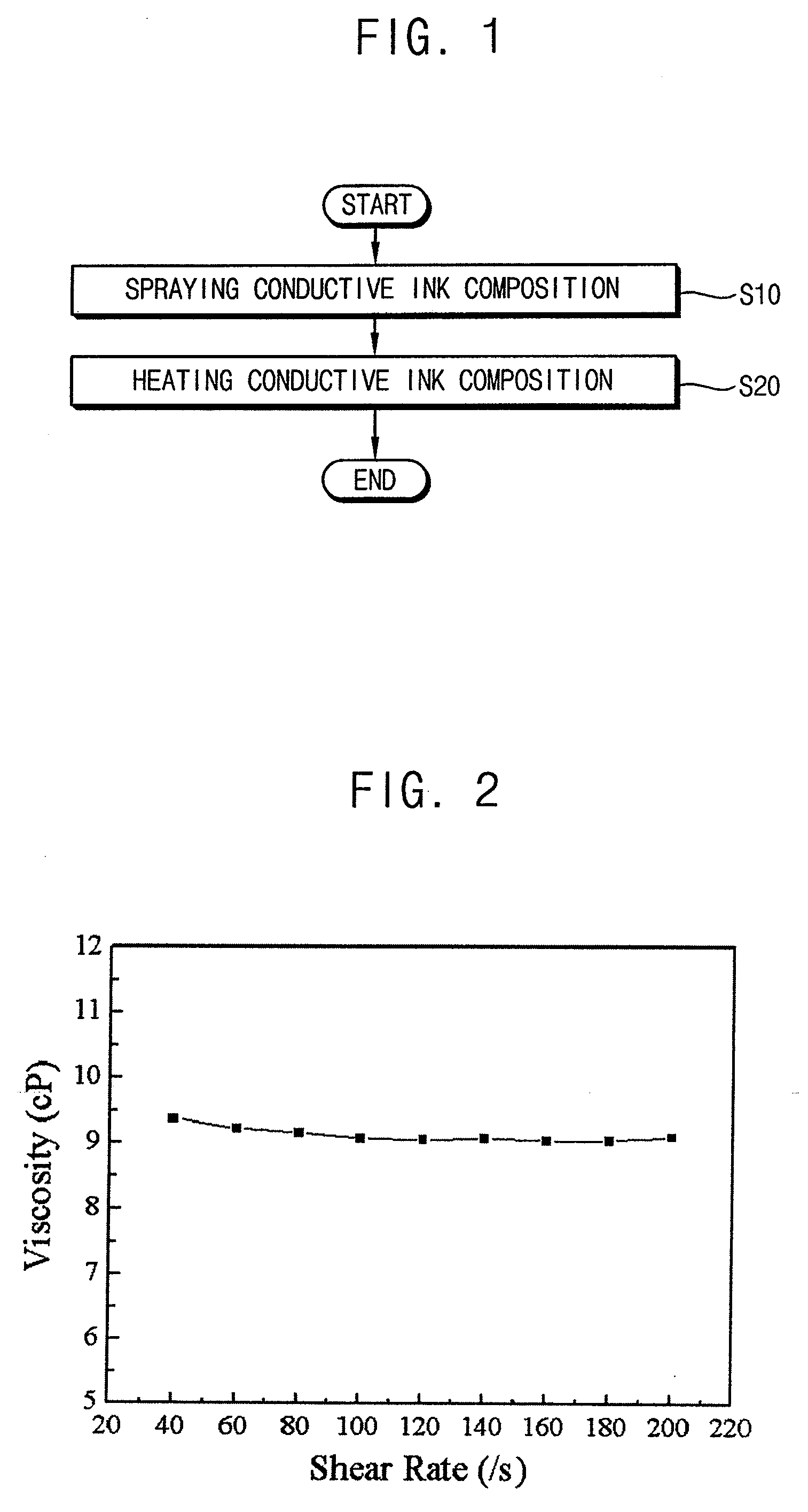
[0030]The invention is described more fully hereinafter with reference to the accompanying drawings, in which exemplary embodiments of the invention are shown. This invention may, however, be embodied in many different forms and should not be construed as limited to the embodiments set forth herein.

[0031]A conductive ink composition according to an exemplary embodiment of the present invention includes about 15% to about 50% by weight of copper nanoparticles, about 40% to about 80% by weight of a non-aqueous solvent mixture, about 0.01% to about 5% by weight of a dispersion agent and about 1% to about 20% by weight of a wetting agent.

[0032]For example, the non-aqueous solvent mixture may include a first solvent, of which a viscosity is about 0.1 mPa·s to about 5 mPa·s at about 25° C., a second solvent, of which a viscosity is about 15 mPa·s to about 40 mPa·s at about 25° C., and a third solvent, of which a vapor pressure is about 10 mmHg to about 250 mmHg at about 25° C. When the co...


PUM

PropertyMeasurementUnit
vapor pressureaaaaaaaaaa
viscosityaaaaaaaaaa
viscosityaaaaaaaaaa

Abstract

A conductive ink composition includes about 15% to about 50% by weight of copper nanoparticles, about 40% to about 80% by weight of a non-aqueous solvent mixture, about 0.01% to about 5% by weight of a dispersion agent and about 1% to about 20% by weight of a wetting agent. A conductive pattern may be formed with use of the conductive ink composition and an inkjet printer.

Description

CROSS-REFERENCE TO RELATED APPLICATION[0001]This application claims priority under 35 USC §119 to Korean Patent Application No. 2007-31284, filed on Mar. 30, 2007 in the Korean Intellectual Property Office (KIPO), the contents of which are herein incorporated by reference in their entirety.BACKGROUND OF THE INVENTION[0002]1. Technical Field[0003]The present invention relates to a conductive ink composition and a method of forming a conductive pattern using the conductive ink composition.[0004]2. Discussion of the Related Art[0005]An optical patterning method using a photolithography process is used for forming a conductive pattern. However, the optical patterning method using the photolithography process requires many processing steps and is complicated, so that the manufacturing costs for forming the conductive pattern are increased. Types of substrates usable in the optical patterning method may be limited due to an exposure process and a development process. Furthermore, environm...

Claims


Application Information

Patent Timeline
Patent Type & Authority Applications(United States)
IPC IPC(8): H01B1/02B05D1/40
CPCC09D11/36C09D11/52H01B1/22H05K1/097C09D11/38H01L21/02
Inventor KIM, JANG SUBLIM, SOON-KWONMOON, JOO-HOJEONG, SUN-HOKIM, DONG-JOWOO, KYOO-HEE
Owner SAMSUNG DISPLAY CO LTD
Why Eureka
Try Eureka