Interconnection, electronic device and method for manufacturing an electronic device

a technology of electronic devices and connectors, applied in the direction of nanoinformatics, semiconductor/solid-state device details, conductors, etc., can solve the problems of reducing the mechanical strength of the plug between the wiring layer, reducing the mechanical strength, and high current density that exceeds the limit of cu material, etc., to suppress performance deterioration and high reliability

Active Publication Date: 2008-10-09
KK TOSHIBA
View PDF4 Cites 17 Cited by
  • Summary
  • Abstract
  • Description
  • Claims
  • Application Information

AI Technical Summary

Benefits of technology

[0011]It is an object of the present invention to provide an interconnection having high reliability and capable of suppressin

Problems solved by technology

However, in the 32 nm half-pitch (HP) technology node, a high current density that exceeds the limit of Cu material is required.
On the other hand, it is difficult to grow the bundle of carbon nanotubes having the high density and fine dimension that is demanded for the 32 nm HP technology node.
The structure of the bundle of low-density carbon nanotubes may possibly decrea

Method used


Image

  • Interconnection, electronic device and method for manufacturing an electronic device
  • Interconnection, electronic device and method for manufacturing an electronic device
  • Interconnection, electronic device and method for manufacturing an electronic device

Examples


Embodiment Construction

[0020]Various embodiments of the present invention will be described with reference to the accompanying drawings. It is to be noted that the same or similar reference numerals are applied to the same or similar parts and elements throughout the drawings, and the description of the same or similar parts and elements will be omitted or simplified.

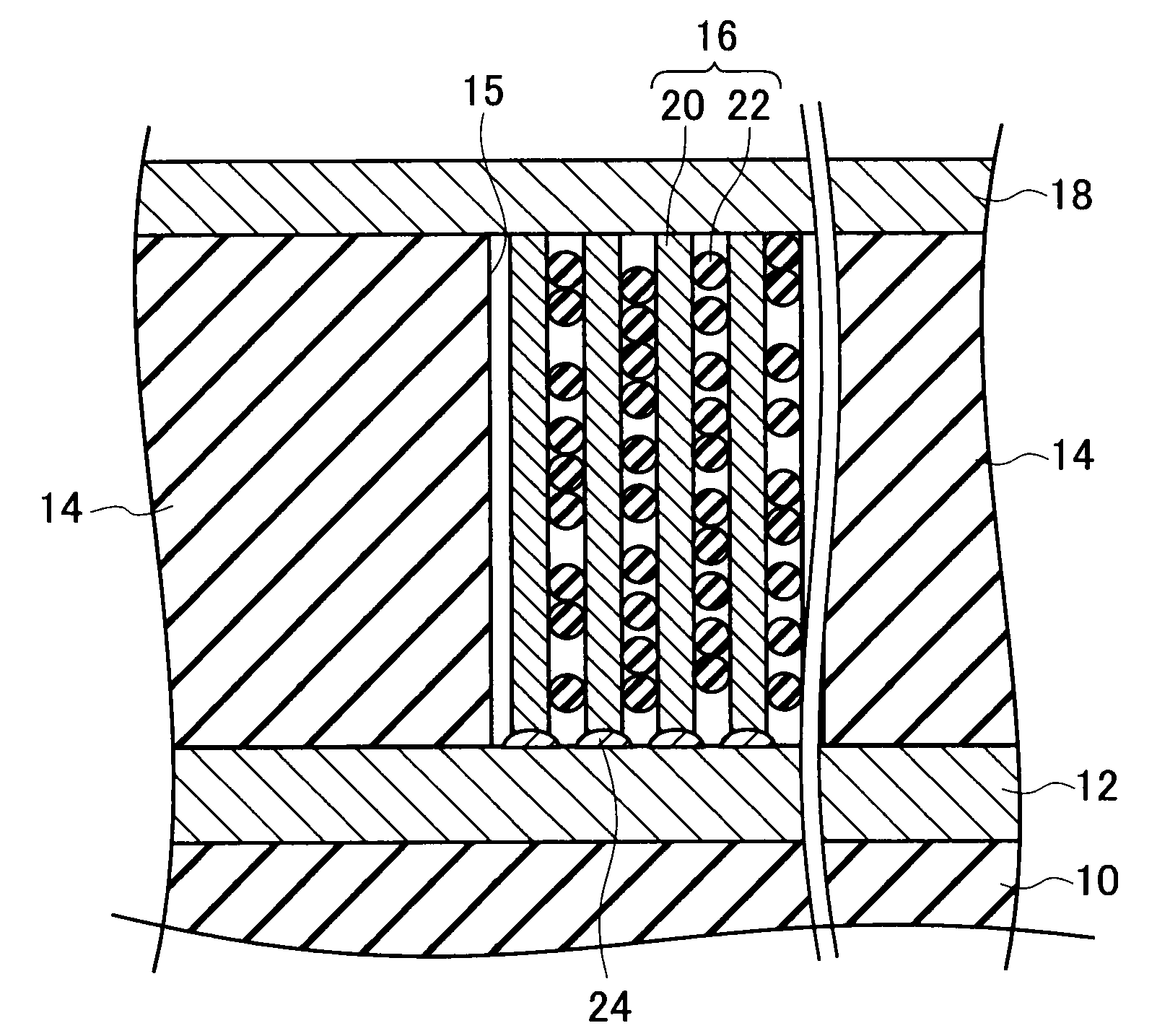
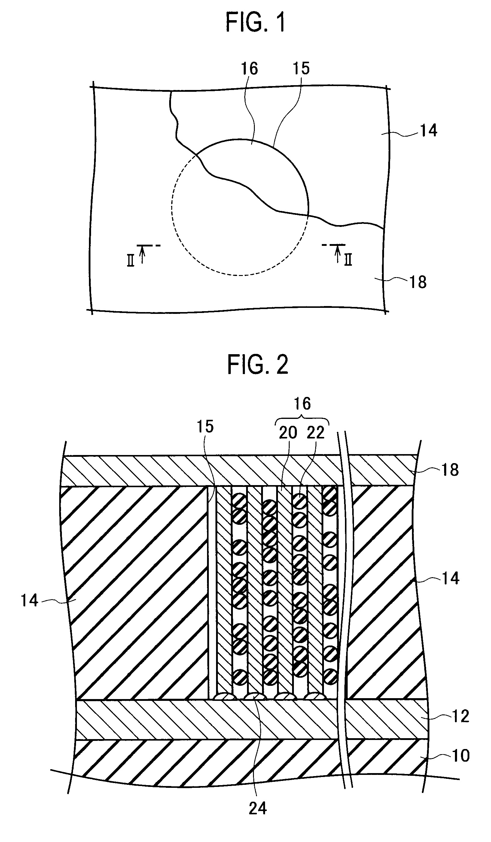
[0021]An electronic device, such as a semiconductor device and the like, according to an embodiment of the present invention, includes a first conductive film (bottom conductive film) 12, an interlevel dielectric film 14, an interconnection (plug) 16, a second conductive film (top conductive film) 18 and the like, on an underlying insulating film 10, as shown in FIGS. 1, 2. Also, the electronic device includes a substrate (not shown) in which transistors and the like are formed, below the underlying insulating film 10. The bottom conductive film 12 is a wiring layer provided on the underlying insulating film 10 and the top conductive film 18 ...


PUM

PropertyMeasurementUnit
Diameteraaaaaaaaaa
Electrical conductoraaaaaaaaaa
Crystal structureaaaaaaaaaa

Abstract

An interconnection includes a bundle of conductive members, each of the conductive members being made of carbon nanotube having an end connected to a first conductive film, and another end connected to a second conductive film separated from the first conductive film; and carbon particles each having a diamond crystal structure, dispersed between the conductive members.

Description

CROSS REFERENCE TO RELATED APPLICATIONS AND INCORPORATION BY REFERENCE[0001]This application is based upon and claims the benefit of priority from prior Japanese Patent Application P2007-099542 filed on Apr. 5, 2007; the entire contents of which are incorporated by reference herein.BACKGROUND OF THE INVENTION[0002]1. Field of the Invention[0003]The present invention relates to an interconnection, an electric device and a method for manufacturing an electric device using a carbon nanotube.[0004]2. Description of the Related Art[0005]In semiconductor devices, such as large-scale integrated circuits (LSIs) and the like, higher integration and miniaturization have advanced year to year, as shown by Moor's law or a semiconductor road map. Along with the advancement of semiconductor devices, interconnections having fine dimension are also required for the semiconductor devices. The interconnection material, which started with aluminum (Al), has been replaced with copper (Cu) due to the de...

Claims


Application Information

Patent Timeline
IPC IPC(8): H05K1/09H01B5/08H05K3/02
CPCB82Y10/00H01L21/288H01L21/76879H01L23/53276H01L2221/1094H05K3/4038Y10T29/49155H05K2201/0323H01L2924/0002Y10S977/742H05K2201/026H01L2924/00
Inventor SAKAI, TADASHISAKUMA, NAOSHIKATAGIRI, MASAYUKIONO, TOMIOSUZUKI, MARIKO
Owner KK TOSHIBA
Why Eureka
Try Eureka