Method of forming a micro pattern of a semiconductor device

Active Publication Date: 2008-10-09
SK HYNIX INC
View PDF3 Cites 19 Cited by
  • Summary
  • Abstract
  • Description
  • Claims
  • Application Information

AI Technical Summary

Benefits of technology

[0004]Accordingly, the present invention addresses the above problems, and discloses a method of forming a micro pattern of a semiconduc

Problems solved by technology

The process method increases not only the overall number

Method used


Image

  • Method of forming a micro pattern of a semiconductor device
  • Method of forming a micro pattern of a semiconductor device
  • Method of forming a micro pattern of a semiconductor device

Examples


first embodiment

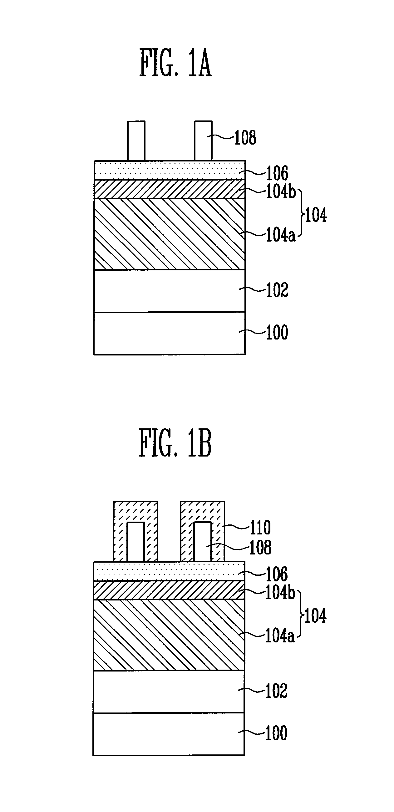
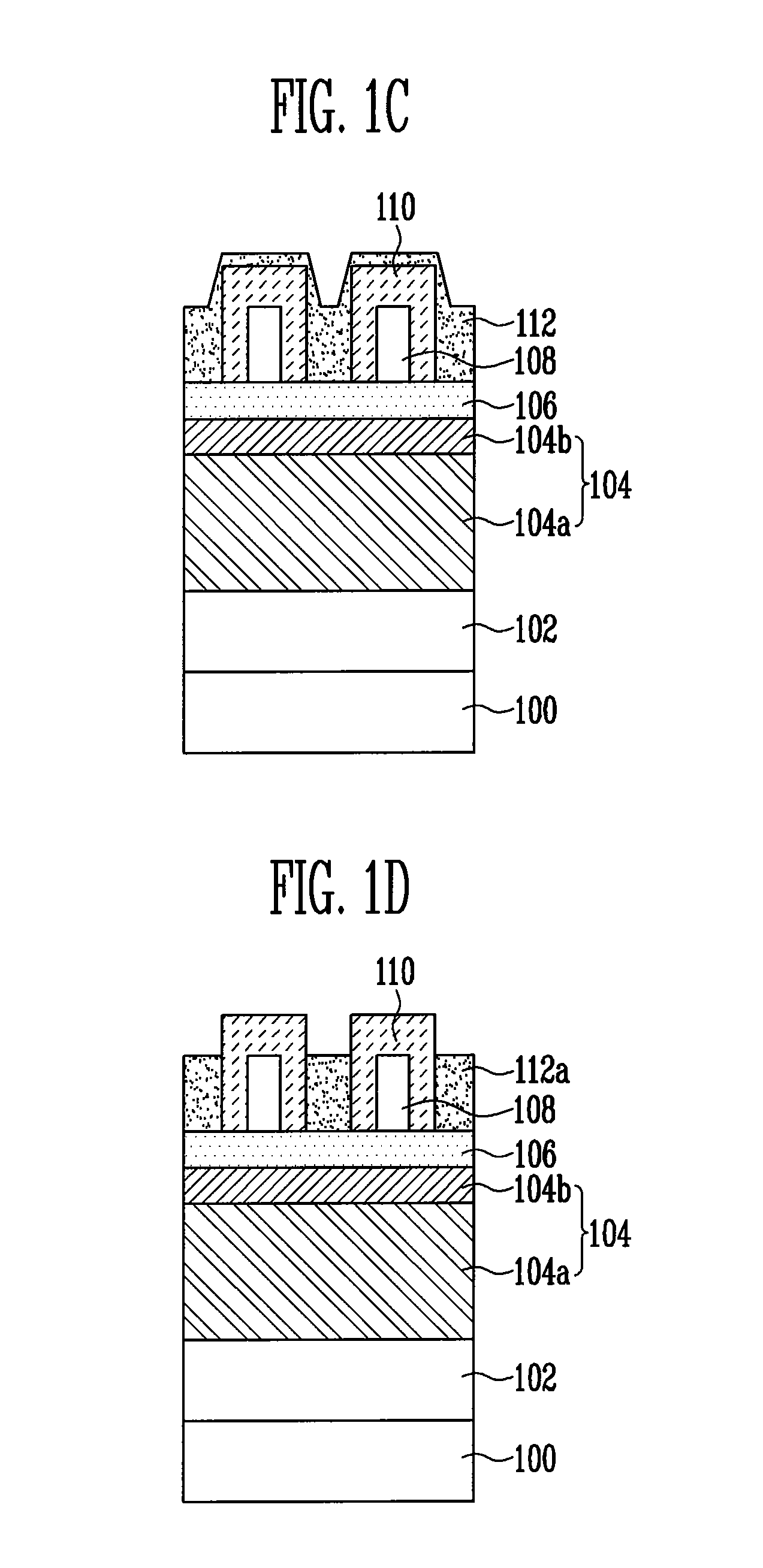
[0012]FIGS. 1A to 1G are cross-sectional views illustrating a method of forming a micro pattern of a semiconductor device according to the present invention. In this method, process steps are performed only on a cell gate region.

[0013]Referring to FIG. 1A, an etch target layer 102 is formed over a semiconductor substrate 100. The etch target layer 102 can be formed as a film, such as an insulating layer, a conductive layer or an interlayer insulating layer. A hard mask layer 104 and a BARC layer 106 are formed over the etch target layer 102. The hard mask layer 104 has a stack structure including an amorphous carbon layer 104a and a silicon oxynitride (SiON) layer 104b. The BARC layer 106 may include silicon (Si).

[0014]Thereafter, a first auxiliary pattern 108 is formed on the BARC layer 106. The first auxiliary pattern 108 may be a photoresist layer or a photoresist layer containing silicon (Si). The Critical Dimension (CD) of the first auxiliary pattern 108 is defined to be approx...

second embodiment

[0026]FIGS. 2A to 2H are cross-sectional views illustrating a method of forming a micro pattern of a semiconductor device according to the present invention.

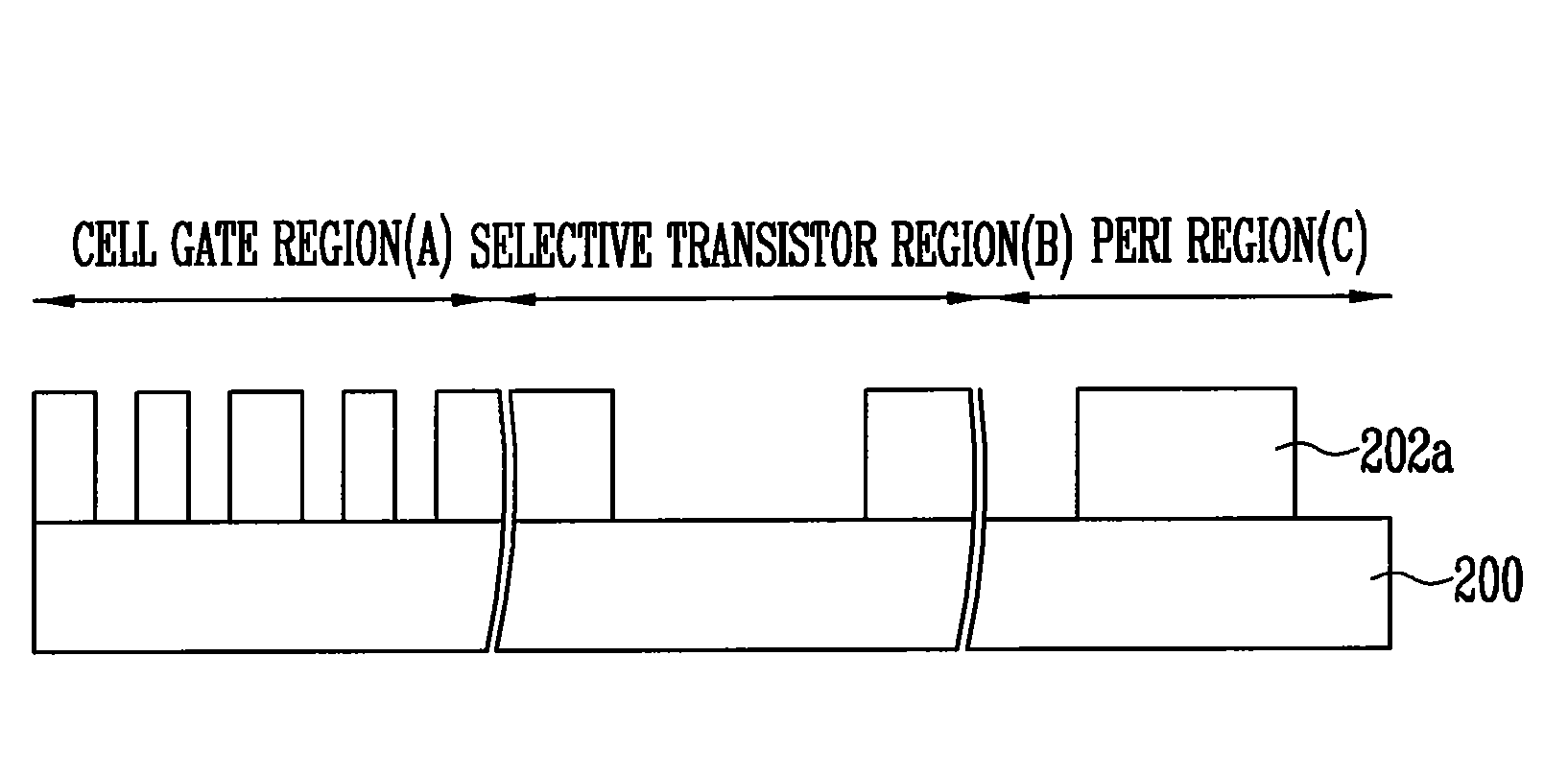
[0027]Referring to FIG. 2A, an etch target layer 202 is formed on a semiconductor substrate 200 having a cell gate region A, a selective transistor region B and a peri region C. The etch target layer 202 is formed of a tungsten silicide (WSix) layer. A stack structure including a tunnel insulating layer, a first conductive layer for a floating gate, a dielectric layer and a second conductive layer for a control gate are formed between the tungsten silicide (WSix) layer and the semiconductor substrate 200.

[0028]Thereafter, a hard mask layer 204 and a BARC layer 206 are formed over the etch target layer 202. The hard mask layer 204 may have a stack structure including an amorphous carbon layer 204a and a silicon oxynitride (SiON) layer 204b, and the BARC layer 206 may be formed using BARC containing silicon (Si).

[0029]Thereafter, ...


PUM

PropertyMeasurementUnit
Thicknessaaaaaaaaaa
Electrical conductoraaaaaaaaaa
Heightaaaaaaaaaa

Abstract

A method of forming a micro pattern of a semiconductor device includes forming an etch target layer, a hard mask layer, a Bottom Anti-Reflective Coating (BARC) layer and a first photoresist pattern over a semiconductor substrate. An organic layer is formed on a surface of the first photoresist pattern. A second photoresist layer is formed over the BARC layer and the organic layer. An etch process is performed so that the second photoresist layer remains on the BARC layer between the first photoresist patterns and becomes a second photoresist pattern. The organic layer on the first photoresist pattern and between the first and second photoresist patterns is removed. The BARC layer formed below the organic layer is removed. The hard mask layer is etched using the first and second photoresist patterns as an etch mask. The etch target layer is etched using a hard mask pattern as an etch mask.

Description

CROSS-REFERENCES TO RELATED APPLICATIONS[0001]The present application claims priority to Korean patent application number 2007-34202, filed on Apr. 6, 2007, which is incorporated by reference in its entirety.BACKGROUND OF THE INVENTION[0002]The present invention relates to semiconductor devices, and more particularly, to a method of forming a micro pattern of a semiconductor device, in which the number of process steps can be reduced during a micro pattern formation process.[0003]As the degree of integration of devices increases, the size of the minimum line width to be implemented is reduced. In order to implement a reduced micro line width due to the high integration of the devices, various process steps are required. To form a hard mask pattern for forming a micro pattern, a mask formation process, a Double Exposure Etch Tech (DEET) method or a spacer formation process having several steps must be carried out. The process method increases not only the overall number of process st...

Claims


Application Information

Patent Timeline
IPC IPC(8): H01L21/461
CPCH01L21/0337H01L21/28123H01L21/31144H01L21/32139H01L27/115H01L27/11526H01L27/11529H10B41/40H10B41/41H10B69/00H01L21/0276
Inventor JUNG, WOO YUNG
Owner SK HYNIX INC
Why Eureka
Try Eureka