Multilayer nanocrystal structure and method for producing the same

Active Publication Date: 2008-10-16
SAMSUNG ELECTRONICS CO LTD
View PDF7 Cites 56 Cited by
  • Summary
  • Abstract
  • Description
  • Claims
  • Application Information

AI Technical Summary

Benefits of technology

[0008]In view of the deficiencies of the prior art, in an embodiment, a multilayer nanocrystal structure with

Problems solved by technology

However, the method for preparing the semiconductor nanocrystal has disadvantages in that relatively small-sized nanocrystals are necessarily used as a core and the small-size nanocrystals disadvantageously aggregate due to their insta

Method used


Image

  • Multilayer nanocrystal structure and method for producing the same
  • Multilayer nanocrystal structure and method for producing the same
  • Multilayer nanocrystal structure and method for producing the same

Examples


example 1

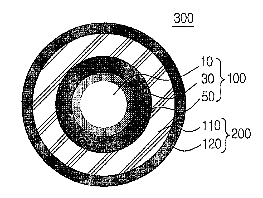
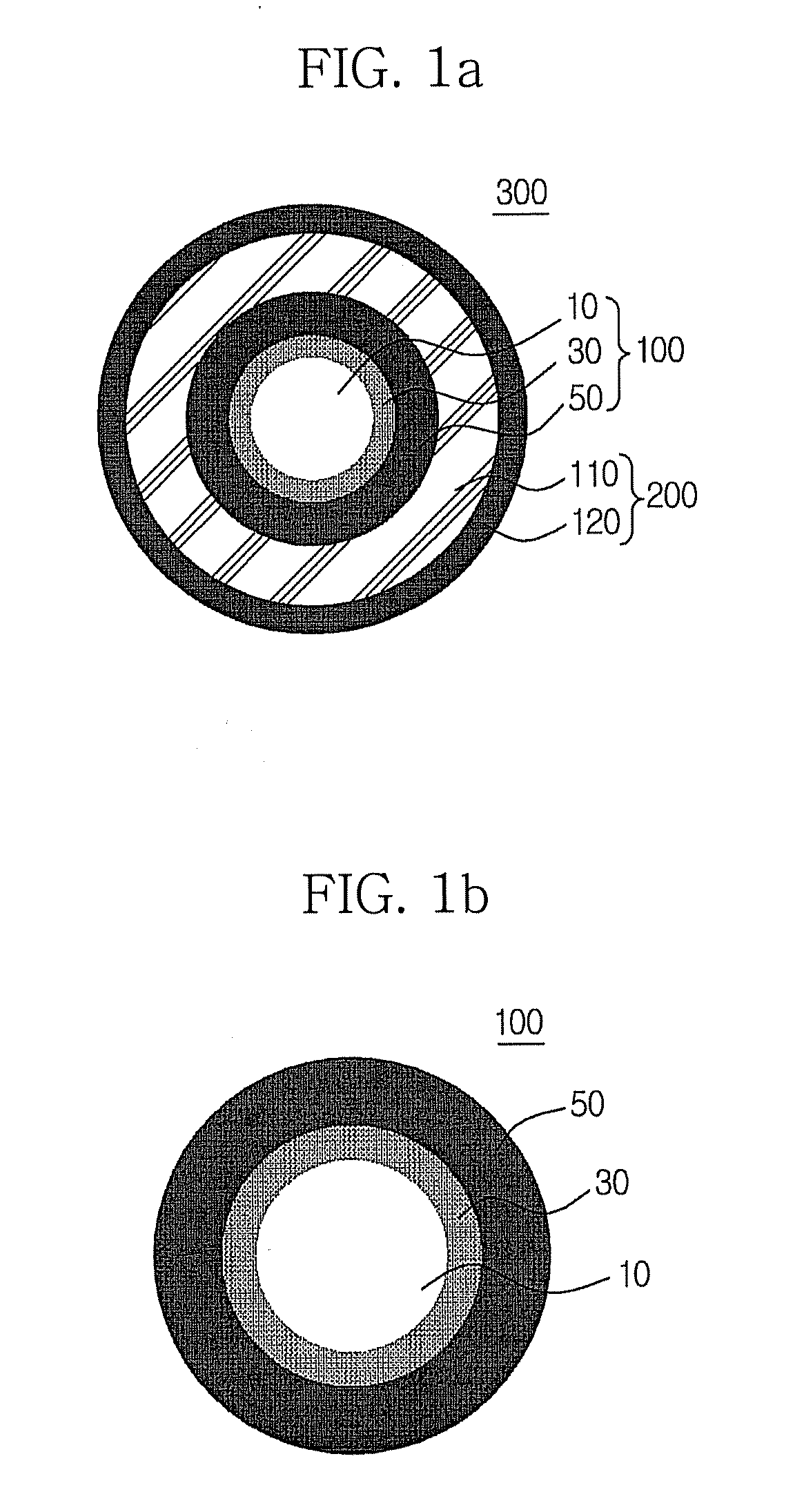
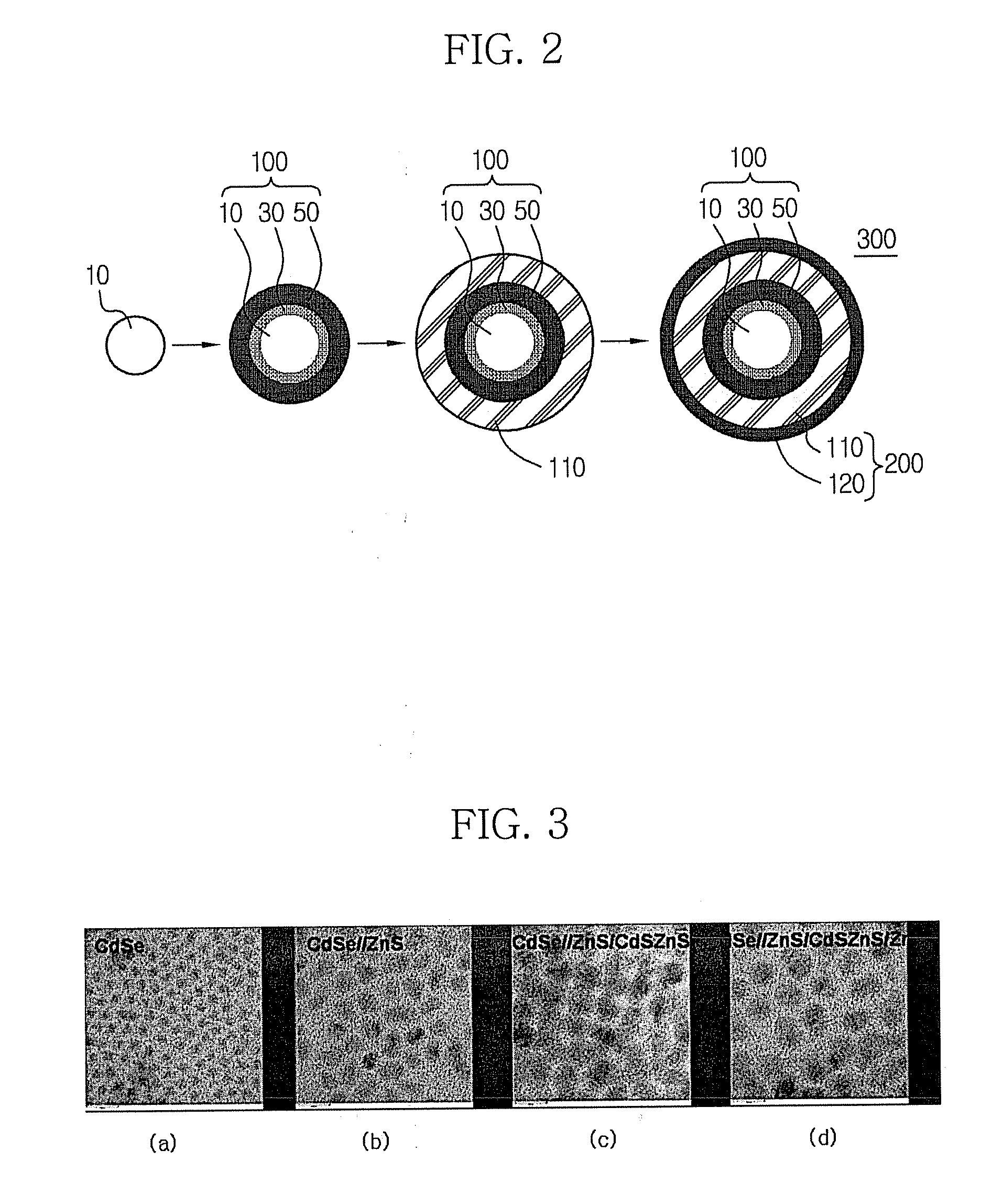
[0069]Production of CdSe / / ZnS / CdSZnS Nanocrystals

[0070]16 g of trioctylamine (hereinafter, referred to as “TOA”), 0.3 g of octadecyl phosphonic acid and 0.4 mmol of cadmium oxide were simultaneously placed in a 125 ml flask equipped with a reflux condenser. The reaction temperature of the mixture was adjusted to 300° C. with stirring.

[0071]Separately, selenium (Se) powder was dissolved in trioctylphosphine (“TOP”) to obtain a Se-TOP complex solution (Se concentration: about 2 M), and 2 ml of the Se-TOP complex solution was rapidly fed to the previous reaction mixture. The reaction was continued for about 2 minutes.

[0072]After completion of the reaction, the reaction mixture was cooled to room temperature as rapidly as possible. Ethanol (10 ml) as a non-solvent was added to the reaction mixture, and then the resulting mixture was centrifuged. The obtained precipitate was separated from the supernatant, and dispersed in toluene (4 ml) to prepare a solution of a CdSe nanocrystal having...

example 2

[0080]Production of CdSe / / ZnS / CdSZnS Nanocrystals with Controlled Band Gap

[0081]8 g of TOA, 0.1 g of oleic acid, 0.1 mmol of cadmium oxide and 0.4 mmol of zinc acetate were simultaneously placed in a 125 ml flask equipped with a reflux condenser. The reaction temperature of the mixture was adjusted to 300° C. with stirring. After 2 ml of the CdSe / / ZnS nanocrystal solution prepared in Example 1 was added to the reaction mixture, 1 ml of an S-TOP complex solution (0.8 M of sulfur in TOP) was slowly added thereto. The reaction was continued for about one hour to grow a CdSZnS nanocrystal on the CdSe / / ZnS nanocrystal to produce a CdSe / / ZnS / CdSZnS nanocrystal that emits light at a wavelength of 554 nm.

[0082]After the reaction was completed, the reaction mixture was cooled to room temperature as rapidly as possible. Ethanol (10 ml) as a non-solvent was added to the reaction mixture, and the resulting mixture was centrifuged. The obtained precipitate was separated from the supernatant, and...

example 3

[0083]Production of CdSe / / ZnS / CdSZnS Nanocrystals According to Changes in Band Gap

[0084]8 g of TOA, 0.1 g of oleic acid, 0.2 mmol of cadmium oxide and 0.4 mmol of zinc acetate were simultaneously placed in a 125 ml flask equipped with a reflux condenser. The reaction temperature of the mixture was adjusted to 300° C. with stirring. After the CdSe / / ZnS nanocrystal solution prepared in Example 1 was added to the reaction mixture, 1 ml of an S-TOP complex solution (0.8 M of sulfur in TOP) was slowly added thereto. The reaction was continued for about one hour to grow a CdSZnS nanocrystal on the CdSe / / ZnS nanocrystal to produce a CdSe / / ZnS / CdSZnS nanocrystal that emits light at a wavelength of 570 nm.

[0085]After the reaction was completed, the reaction mixture was cooled to room temperature as rapidly as possible. Ethanol (10 ml) as a non-solvent was added to the reaction mixture, and the resulting mixture was centrifuged. The obtained precipitate was separated from the supernatant, and...


PUM

PropertyMeasurementUnit
Band gapaaaaaaaaaa

Abstract

Disclosed herein is a multilayer nanocrystal structure comprising a nanocrystal alloy core comprising two or more nanocrystals and including an alloy interlayer formed at an interface between the two or more nanocrystals, and one or more layers of nanocrystal shells formed sequentially on the surface of the nanocrystal alloy core, wherein the nanocrystal shells each have different band gaps. The multilayer nanocrystal structure can be applied to various electronic devices owing to its advantages of high luminescence efficiency, superior optical stability, and superior chemical stability.

Description

[0001]This non-provisional application claims priority to Korean Patent Application No. 10-2007-0029183, filed on Mar. 26, 2007, and all the benefits accruing therefrom under 35 U.S.C. § 119(a), the content of which is herein incorporated by reference in its entirety.BACKGROUND OF THE INVENTION[0002]1. Field of the Invention[0003]The present invention relates to a multilayer nanocrystal structure and a method for producing a multilayer nanocrystal structure. More specifically, the present invention relates to a multilayer nanocrystal structure with high luminescence efficiency, superior optical stability and superior chemical stability, the multilayer nanocrystal structure comprising: a nanocrystal alloy core including an alloy interlayer, two or more nanocrystals formed at the interface between the two or more nanocrystals, and one or more layers of nanocrystal shells formed sequentially on a surface of the nanocrystal alloy core; and a method for producing the multilayer nanocryst...

Claims


Application Information

Patent Timeline
IPC IPC(8): H01J1/32B32B15/02B05D5/12
CPCC30B7/14C30B29/40Y10T428/2989C30B29/605C30B29/48Y02E10/50Y02B10/10B82B1/00H05B33/02B82B3/00H01L31/04
Inventor JANG, EUN JOOJUN, SHIN AELIM, JUNG EUNCHOI, HYE RAN
Owner SAMSUNG ELECTRONICS CO LTD
Why Eureka
Try Eureka