Semiconductor memory device

a memory device and semiconductor technology, applied in the field of semiconductor memory devices, can solve the problems of difficult to amplify a minute potential difference, long length of bit lines, and performance problems, and achieve the effects of reducing the size of memory cells, and suppressing the increase in the entire area

Active Publication Date: 2008-10-16
LONGITUDE LICENSING LTD
View PDF5 Cites 38 Cited by
  • Summary
  • Abstract
  • Description
  • Claims
  • Application Information

AI Technical Summary

Benefits of technology

[0022]As described above, according to the present invention, by employing a hierarchical memory cell array, the local bit lines each partitioned into N sections along the global bit line are arranged, and the entire semiconductor memory device is configured using the single-ended local sense amplifiers corresponding to the local bit lines and using the single-ended global sense amplifiers corresponding to the global bit lines. Thus, memory cells can be arranged at all intersections of local bit lines having

Problems solved by technology

In recent years, as the capacity of the DRAM becomes large, an extremely large number of memory cells are connected to each bit line, thereby causing performance problems due to an increase in parasitic capacitance and resistance of the bit line.
As described above, when employing the single-ended sense amplifiers, it is difficult to amplify a minute potential difference, as different from using the differential sense amplifiers.
On the other hand, in th

Method used


Image

  • Semiconductor memory device
  • Semiconductor memory device
  • Semiconductor memory device

Examples


first embodiment

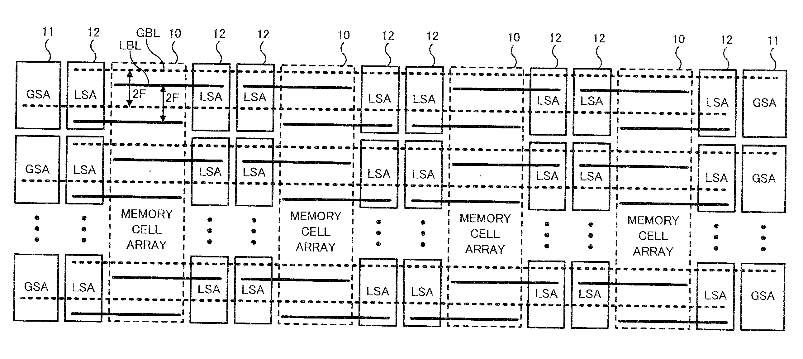
[0059]A first embodiment of the present invention will be described. FIG. 1 shows an entire configuration of a DRAM of the first embodiment. In FIG. 1, there are shown four memory cell arrays 10, a plurality of global sense amplifiers 11, a plurality of local sense amplifiers 12, a plurality of global bit lines GBL, and a plurality of local bit lines LBL.

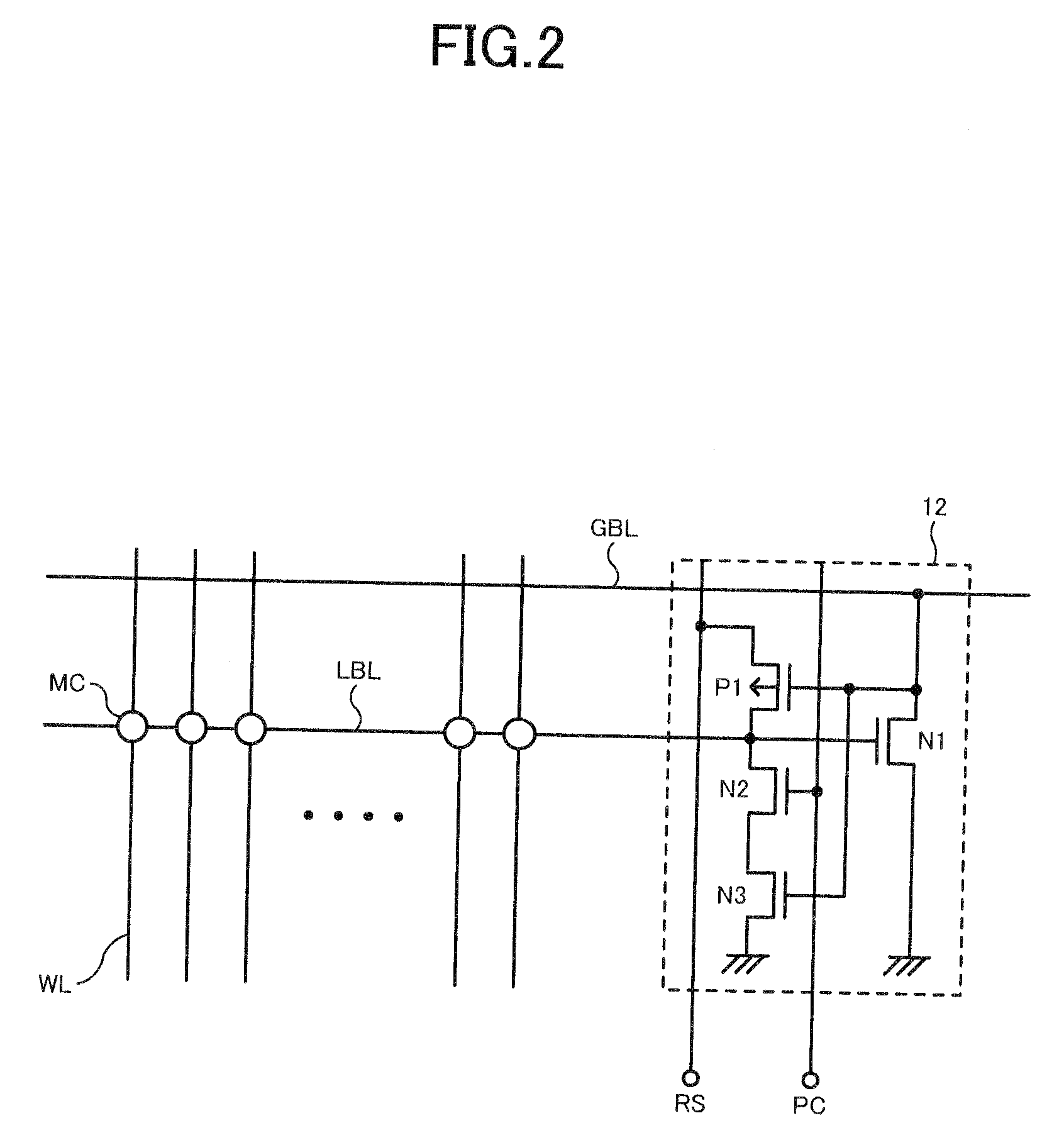
[0060]Each memory cell array 10 includes a large number of memory cells (not shown) formed at all intersections of a plurality of word lines (not shown) and a plurality of local bit lines LBL intersecting therewith. For example, by arranging M word lines WL and N local bit lines LBL in one memory cell array 10, the memory cell array 10 becomes capable of storing M×N bit data and the entire storage capacity of the DRAM is 4×M×N bits. As shown in FIG. 1, the plurality of local bit lines LBL is regularly aligned with a pitch 2F based on a design rule value F in a word line extending direction. Besides, the plurality of global bit lines...

second embodiment

[0089]A second embodiment of the present invention will be described. The entire configuration of a DRAM of the second embodiment is the same as the first embodiment (FIG. 1), so description thereof is omitted. FIG. 7 shows a configuration example of the local sense amplifier 12 of the second embodiment. The local sense amplifier 12 of FIG. 7 is a single-ended sense amplifier including four NMOS transistor N11, N12, N13 and N14. In the second embodiment, since the local sense amplifier 12 is configured using only NMOS transistors without using PMOS transistors, a well for separating PMOS and NMOS areas is not required, so that the layout area of the local sense amplifier 12 can be further reduced.

[0090]In FIG. 7, the NMOS transistor N11 is connected between the global bit line GBL and ground in the same manner as the NMOS transistor N1 of FIG. 2. Meanwhile, the NMOS transistor N12 is connected between the gate of the NMOS transistor N11 and ground, and the NMOS transistor N13 is con...

third embodiment

[0107]A third embodiment of the present invention will be described. The entire configuration of a DRAM of the third embodiment is the same as the first embodiment (FIG. 1), so description thereof is omitted. FIG. 12 shows a configuration example of the local sense amplifier 12 of the third embodiment. The local sense amplifier 12 of FIG. 12 is a single-ended sense amplifier including four NMOS transistor N21, N22, N23 and N24. In the third embodiment, it is common to the second embodiment that the layout area can be reduced by configuring the local sense amplifier 12 using only NMOS transistors, however its circuit configuration is different.

[0108]In FIG. 12, NMOS transistor N21, N23 and N24 have the same functions as those of the NMOS transistor N11, N12 and N14 of FIG. 7. Meanwhile, the NMOS transistor 13 of FIG. 7 is not provided, and the NMOS transistor N22 is connected between the global bit line GBL and the NMOS transistor N21. The control signal line RT is connected to the g...


PUM


Abstract

A semiconductor memory device comprises word lines, global bit lines intersecting with the word lines; local bit lines partitioned into N sections along the global bit lines and aligned with a same pitch as the global bit lines; N memory cell arrays each including memory cells formed at intersections of the word lines and the local bit lines and being arranged corresponding to the sections of the local bit lines; local sense amplifiers for amplifying a signal read out from a selected memory cell to the local bit line and for outputting the signal to the global bit line; global sense amplifiers for amplifying the signal transmitted from the local sense amplifier corresponding to the selected memory cell through the global bit line and for selectively coupling the signal to an external data line.

Description

BACKGROUND OF THE INVENTION[0001]1. Field of the Invention[0002]The present invention relates to a semiconductor memory device which rewritably stores data in a plurality of memory cells formed at intersections of a plurality of word lines and a plurality of bit lines, and particularly relates to a semiconductor memory device in which a memory cell array having a hierarchical structure is configured with a unit including a predetermined number of local bit lines and one global bit line.[0003]2. Description of the Related Art[0004]In a general DRAM, there are provided a memory cell array including memory cells formed at intersections of bit lines and word lines, and a large number of sense amplifiers for amplifying data of the memory cells. In recent years, as the capacity of the DRAM becomes large, an extremely large number of memory cells are connected to each bit line, thereby causing performance problems due to an increase in parasitic capacitance and resistance of the bit line. ...

Claims


Application Information

Patent Timeline
IPC IPC(8): G11C5/02G11C5/06
CPCG11C5/025G11C5/063G11C7/067G11C7/1051G11C7/1069G11C11/4097G11C7/1096G11C7/18G11C11/4091G11C11/4096G11C7/1078
Inventor KAJIGAYA, KAZUHIKO
Owner LONGITUDE LICENSING LTD
Why Eureka
Try Eureka