Semiconductor device and manufaturing method thereof

a technology of semiconductor devices and semiconductors, applied in semiconductor devices, basic electric elements, electrical equipment, etc., can solve the problems of increased power consumption, inability to perform high-speed operation, and inability to operate normally of semiconductor devices, so as to achieve the effect of reducing power consumption, reducing the resistance of wirings that connect between the lower diffusion layer and substantially reducing the resistance of wirings

Inactive Publication Date: 2008-10-23
ELPIDA MEMORY INC
View PDF5 Cites 23 Cited by
  • Summary
  • Abstract
  • Description
  • Claims
  • Application Information

AI Technical Summary

Benefits of technology

[0015]As described above, a semiconductor device according to one aspect of the present invention includes plural lower electrodes that mutually short-circuit lower diffusion layers adjacent to a first direction. Therefore, the wiring resistance of wirings that connect between the lower diffusion layers can be substantially decreased. As a result, when a memory cell array is configured having bit lines at the lower diffusion layer side, for example, power consumption can be decreased by decreasing the bit line resistance, and a high-speed operation can be achieved.
[0016]In a semiconductor device accord

Problems solved by technology

When a transistor size is decreased any more, there is a risk that the transistors cannot operate normally due to short channel effect or the like.
Consequently, because the diffusion layer resistance limits the connection resistance of the lower diffusion layers, power consump

Method used


Image

  • Semiconductor device and manufaturing method thereof
  • Semiconductor device and manufaturing method thereof
  • Semiconductor device and manufaturing method thereof

Examples


first embodiment

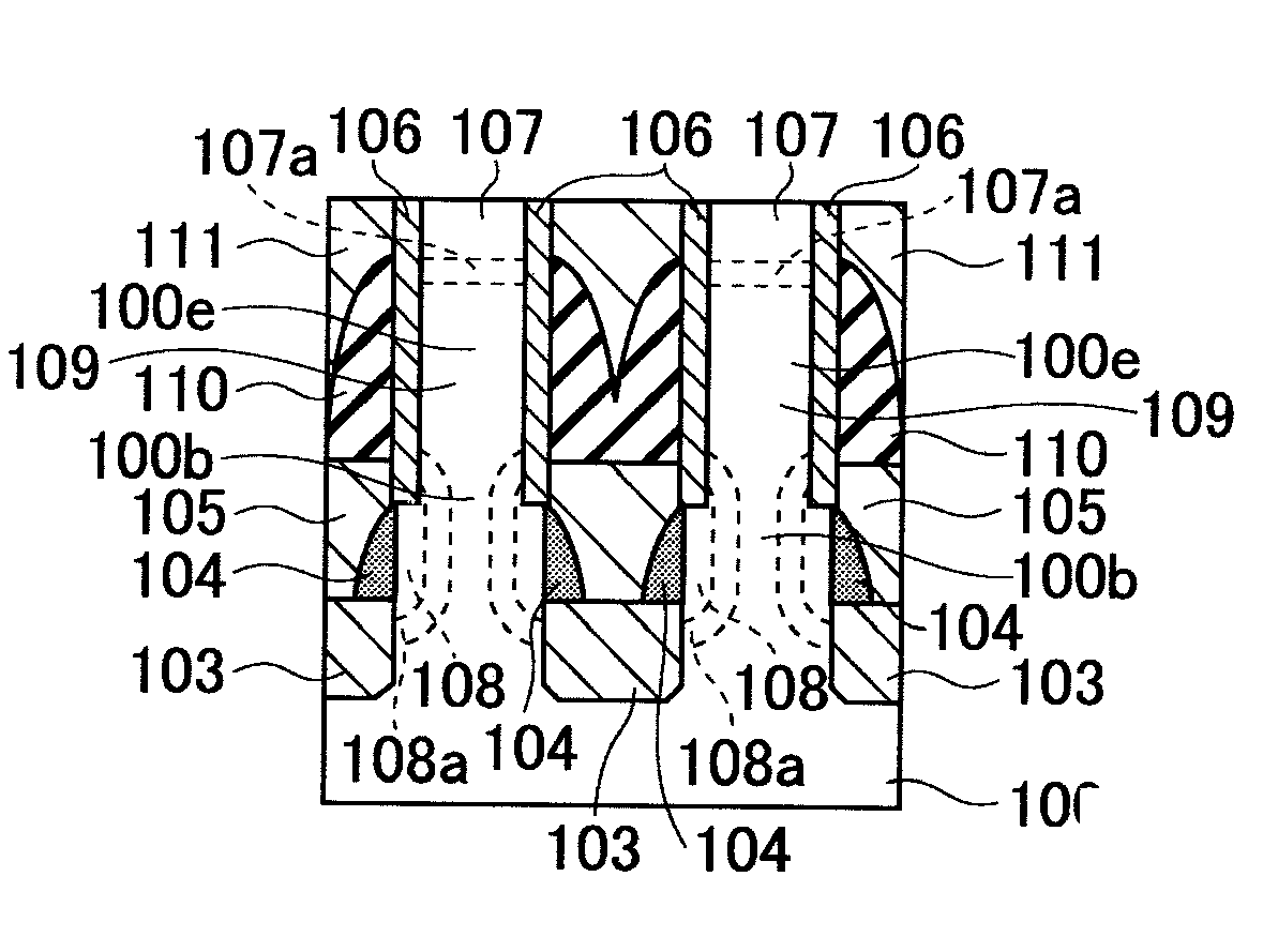
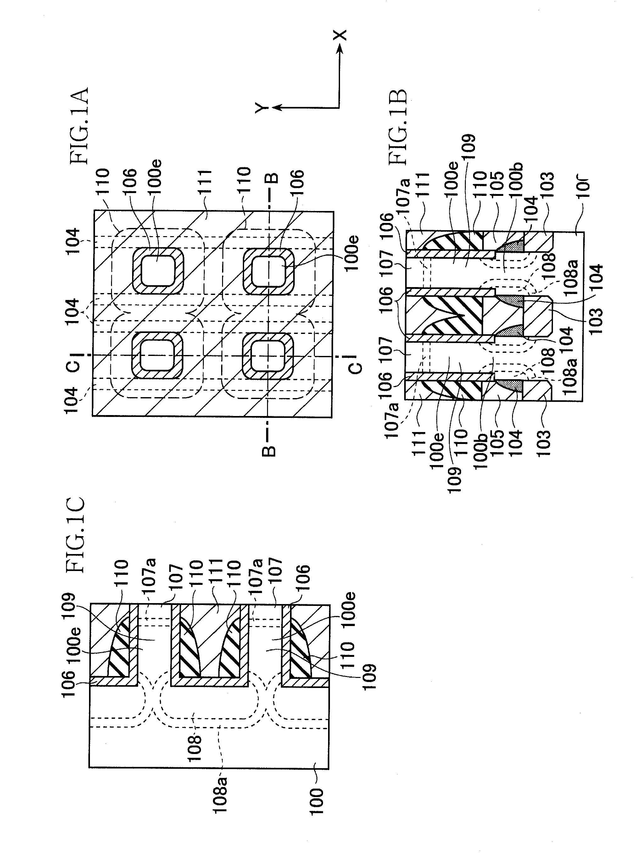
[0050]FIGS. 1A to 1C show relevant parts of a semiconductor device according to the present invention. FIG. 1A is a top plan view of the semiconductor device, FIG. 1B is a cross-sectional view of FIG. 1A cut along a line B-B, and FIG. 1C is a cross-sectional view of FIG. 1A cut along a line C-C.

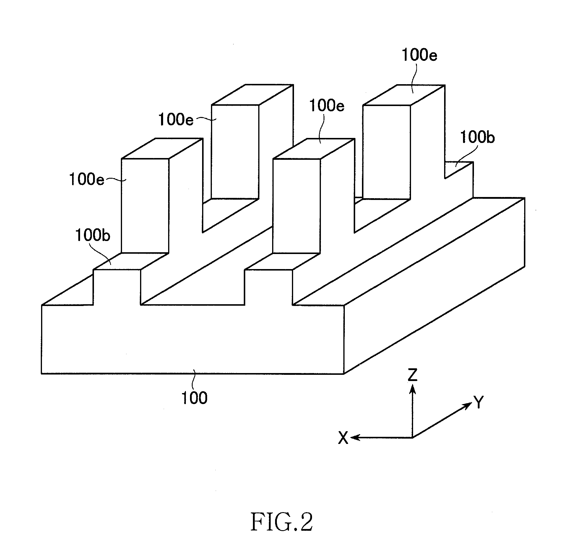
[0051]As shown in FIGS. 1A to 1C, the semiconductor device according to the first embodiment includes a plurality of semiconductor pillars 100e disposed in matrix in the X direction and the Y direction parallel with the main surface of a semiconductor substrate 100. The semiconductor pillars 100e are a part of the semiconductor substrate 100, and are extended to a direction perpendicular to the main surface of the semiconductor substrate 100. An upper diffusion layer 107 is formed in an upper part of each semiconductor pillar 100e, and a lower diffusion layer 108 is formed in a lower part of the semiconductor pillar 100e. Side surface of the semiconductor pillar 100e is covered with a gate in...

second embodiment

[0083]the present invention is explained next.

[0084]FIGS. 17A to 17C show relevant parts of a semiconductor device according to the second embodiment. FIG. 17A is a top plan view of the semiconductor device, FIG. 17B is a cross-sectional view of FIG. 17A cut along the line B-B, and FIG. 17C is a cross-sectional view of FIG. 17A cut along the line C-C. FIG. 18 is a schematic perspective view for explaining the shape of the semiconductor substrate 100 according to the second embodiment.

[0085]As shown in FIGS. 17A to 17C and FIG. 18, in the semiconductor device according to the second embodiment, the projections 100b provided on the semiconductor substrate 100 have island shapes, and are laid out in matrix to the X direction and the Y direction. Each one of semiconductor pillars 100e is provided for each one of island-shaped projections 100b. The planar shape of the projection 100b has an elliptical shape having a larger diameter in the Y direction than a diameter in the X direction. T...


PUM


Abstract

A semiconductor device comprises a plurality of semiconductor pillars laid out in matrix in a first and a second directions parallel with a main surface of a semiconductor substrate, and extending to a direction substantially perpendicular to the main surface; gate insulating films covering each surface of the plurality of semiconductor pillars, respectively; upper diffusion layers formed in each upper part of the plurality of semiconductor pillars, respectively; lower diffusion layers formed in each lower part of the plurality of semiconductor pillars, respectively; gate electrodes encircling at least each channel region between each upper diffusion layer and each lower diffusion layer, respectively; and a plurality of lower electrodes short-circuiting the lower diffusion layers adjacent in the first direction.

Description

TECHNICAL FIELD[0001]The present invention relates to a semiconductor device and a manufacturing method thereof, and more particularly to a semiconductor device having plural transistors laid out in matrix, and a manufacturing method thereof.BACKGROUND OF THE INVENTION[0002]Integration of a semiconductor device has so far been achieved by mainly miniaturization of transistors. Miniaturization of transistors has substantially reached a limit. When a transistor size is decreased any more, there is a risk that the transistors cannot operate normally due to short channel effect or the like.[0003]In order to fundamentally solve these problems, there have been proposed methods of three-dimensionally forming transistors, by three-dimensionally processing a semiconductor substrate. Among transistors formed by these methods, a three-dimensional transistor, using a semiconductor pillar extending in a perpendicular direction to the main surface of the semiconductor substrate as a channel, has ...

Claims


Application Information

Patent Timeline
IPC IPC(8): H01L29/78H01L21/336
CPCH01L27/10876H01L29/0657H01L29/1045H01L29/1083H01L29/41741H01L29/66666H01L29/7827H10B12/053
Inventor OYU, KIYONORI
Owner ELPIDA MEMORY INC
Why Eureka
Try Eureka