Methods, structures and sytems for an image sensor device for improving quantum efficiency of red pixels

Active Publication Date: 2008-10-30
APTINA IMAGING CORP
View PDF3 Cites 35 Cited by
  • Summary
  • Abstract
  • Description
  • Claims
  • Application Information

AI Technical Summary

Benefits of technology

[0008]Still another area of focus in CMOS image sensors is the desired reduction of floating body effects when n-type substrates (such as an n-tub as disclosed in U.S. Patent Application Publication US 2005/0133825 A1) are implemented under the image sensor pixel's photosensor (e.g. photodiode). Floating body effects occur when the pixel is grounded only at the edge of the array, so the pixels in the center of the array exhibit an un

Problems solved by technology

However the CMOS image sensor is susceptible to the generation of dark current that is generally attributed to leakage in the charge collection region of the pinned photodiode, which is strongly dependent on the doping implantation conditions of the CMOS image sensor.
In addition, defects and trap sites inside or near the photodiode depletion region strongly influence the magnitude of dark current generated.
Dark current is but one of the inherent operational challenges in CMOS image sensors, as another area of focus is maximizing the fill factor as pixel size decreases.
Low fill factors can result in a significant

Method used


Image

  • Methods, structures and sytems for an image sensor device for improving quantum efficiency of red pixels
  • Methods, structures and sytems for an image sensor device for improving quantum efficiency of red pixels
  • Methods, structures and sytems for an image sensor device for improving quantum efficiency of red pixels

Examples


first embodiment

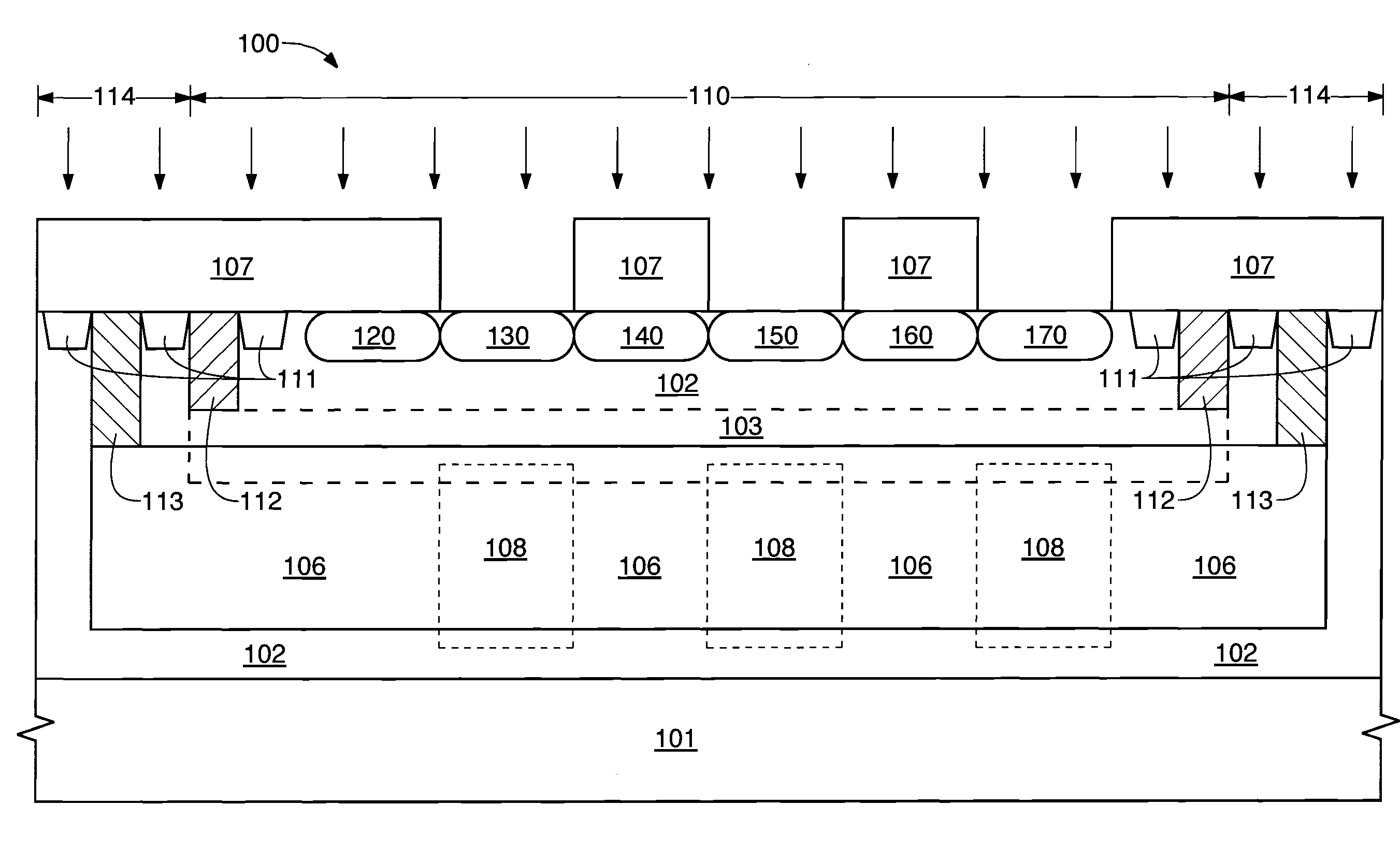
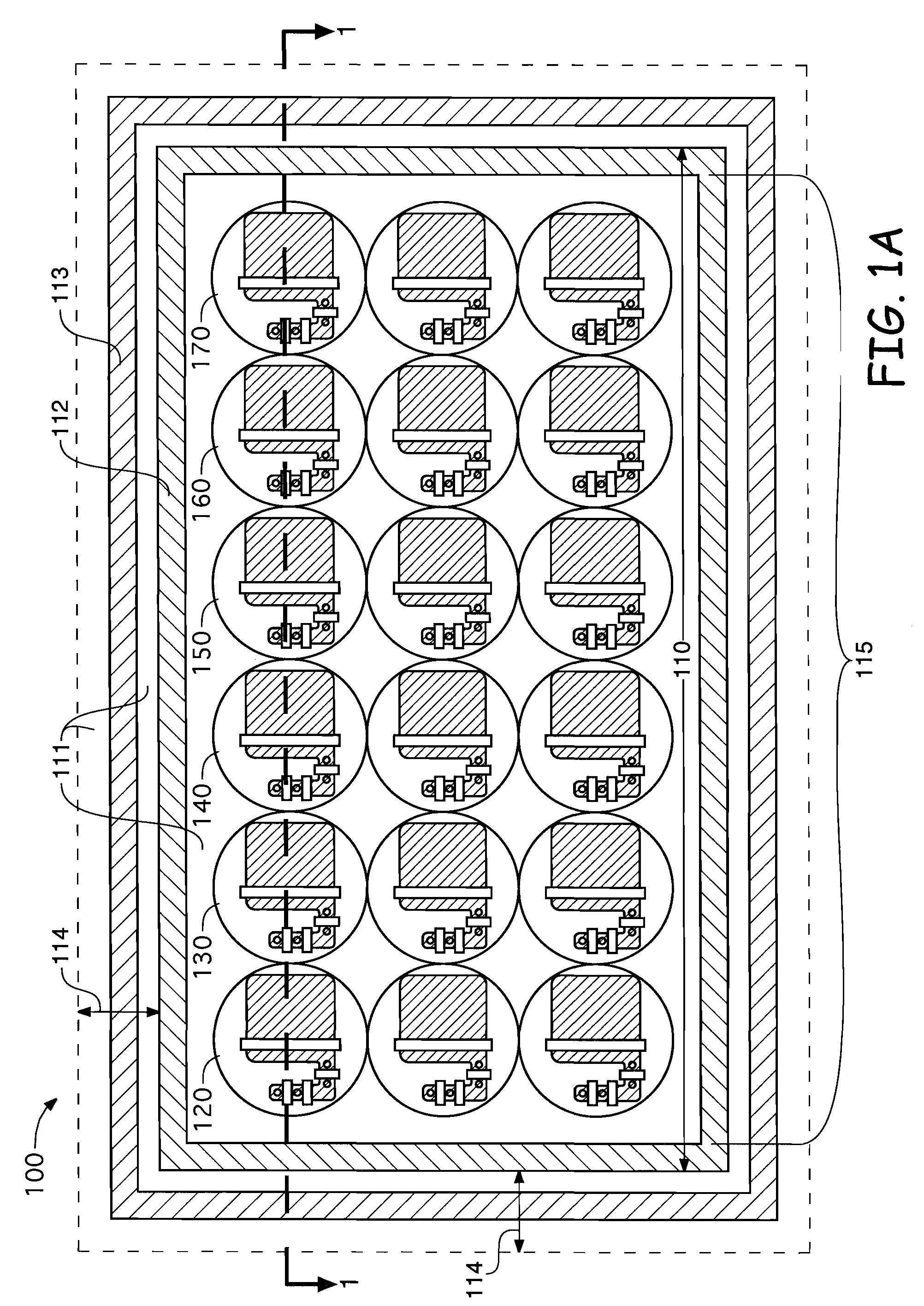
[0023]A CMOS image sensor device in accordance with the present disclosure is fabricated as depicted in the cross-sectional views of FIG. 1C-1E, that correspond to the generally layout of top down view FIG. 1A and in accordance to the cross-sectional view taken along line 1-1 of FIG. 1A.

[0024]Referring now to FIG. 1C, CMOS image sensor 100 utilizes p-type substrate section 101. A p-type epitaxial material is grown in the course of epitaxial deposition and then patterned to form p-type epitaxial region 102 on p-type substrate 101 at a thickness of approximately 4 μm and doped to a p-type conductivity using, for example, boron at a concentration of approximately 7E14 atoms cm−1.

[0025]Next, field oxide regions 111, such as by using shallow trench isolation (STI) techniques know to one skilled in the art, are formed in p-type epitaxial region 102. For example field oxide regions 111 can be formed using a conventional STI process and are typically formed by etching a trench in the substr...

second embodiment

[0031]A CMOS image sensor device in accordance with the present disclosure is fabricated as depicted in the cross-sectional views of FIG. 2C-2D, that correspond to the generally layout of top down view FIG. 1A and in accordance to the cross-sectional view taken along line 1-1 of FIG. 1A.

[0032]Referring now to FIG. 2C, CMOS image sensor 200 utilizes an n-type substrate section 201. An n-type epitaxial material is grown in the course of epitaxial deposition and then patterned to form n-type epitaxial region 202 on n-type substrate 201 at a thickness of approximately 4 μm and doped to a n-type conductivity using for example 4 ohms−em at a concentration of approximately 1E15 atoms cm−3.

[0033]Next, field oxide regions 211, such as by using shallow trench isolation (STI) techniques know to one skilled in the art, are formed in n-type epitaxial region 202. For example field oxide regions 211 can be formed using a conventional STI process and are typically formed by etching a trench in the ...


PUM


Abstract

A method and structure for providing a high energy implant in only the red pixel location of a CMOS image sensor. The implant increases the photon collection depth for the red pixels, which in turn increases the quantum efficiency for the red pixels. In one embodiment, a CMOS image sensor is formed on an p-type substrate and the high energy implant is a p-type implant that creates a p-type ground contact under the red pixel, thus reducing dark non-uniformity effects. In another embodiment, a CMOS image sensor is formed on an n-type substrate and a high energy p-type implant creates a p-type region under only the red pixel to increase photon collection depth, which in turn increases the quantum efficiency for the red pixels.

Description

TECHNICAL FIELD[0001]This invention relates to semiconductor imaging devices and fabrication methods thereof and more specifically to imaging arrays and methods for forming same.BACKGROUND[0002]In general, a Complimentary Metal Oxide Semiconductor (CMOS) image sensor circuit includes a focal plane array of pixels, each one of the pixels includes a photo-conversion device, e.g., a photogate, photoconductor, or photodiode having an associated charge accumulation region within a substrate for accumulating photo-generated charge. Each pixel may include a transistor for transferring charge from the charge accumulation region to a diffusion node and a transistor for resetting the diffusion node to a predetermined charge level prior to charge transference. The pixel may also include a source follower transistor for receiving and amplifying charge from the diffusion node and an access transistor for controlling the readout of the pixel contents from the source follower transistor. In some a...

Claims


Application Information

Patent Timeline
IPC IPC(8): H01L31/042H01L31/18
CPCH01L27/14603H01L27/1463H01L27/14689
Inventor BRADY, FREDERICK T.
Owner APTINA IMAGING CORP
Why Eureka
Try Eureka