
Semiconductor device having plural dram memory cells and a logic circuit and method for manufacturing the same

a memory cell and semiconductor technology, applied in semiconductor devices, semiconductor/solid-state device details, electrical apparatus, etc., can solve the problems of limited capacity of memory mountable on one lsi chip, high cost, and first issue considered problematic, and achieve low cost, low voltage, and ultra-high integration

Inactive Publication Date: 2008-10-30
RENESAS ELECTRONICS CORP
View PDF16 Cites 28 Cited by
  • Summary
  • Abstract
  • Description
  • Claims
  • Application Information

AI Technical Summary

Benefits of technology

This approach results in a highly integrated, low-cost on-chip memory with improved low-voltage operability and reduced manufacturing complexity, enabling efficient co-integration with digital and analog circuitry without the need for additional voltage supply circuits.

Problems solved by technology

However, the cell area is large so that the capacity of a memory mountable on one LSI chip is limited.
However, this results in an increase in process steps for fabrication of 3D structured capacitors; thus, there is a disadvantage that the cost becomes higher.
Furthermore, a second issue is to enable achievement of a low-voltage operation with 1V or below in the above-noted onchip memory.
In addition, a third issue is to realize an on-chip memory suitable also for co-integration with not only digital logic circuitry but also analog circuitry.
The first issue is deemed problematical even at the present time as described in the explanation of the prior art.
This can be said because if the memory unit fails to offer low-voltage operability then it becomes a must to supply different voltages to the logic unit and the memory unit, resulting in incapability to further lower the power consumption of the memory unit.
Unfortunately, an operation at low voltages would result in occurrence of various problems.
Accordingly, when reducing the operating voltage, it becomes difficult to acquire the read signal amount.
However, any one of the both results in an increase in area, which spoils the high integrability.
In addition, the operation of a sense amplifier also becomes difficult.
In particular, with the prior art configuration, the operation at a voltage of about 1V or less is unrealistic.
Therefore, in the case of integrating an onchip memory of large capacity together with a large-scale digital circuit and analog circuit, various kinds of fabrication steps are added, resulting in occurrence of anxiety as to an increase in manufacturing process cost.
Another anxiety lies in a decrease in performance, reliability or manufacturing yield due to the combination of different kinds of processes.

Method used


Image

  • Semiconductor device having plural dram memory cells and a logic circuit and method for manufacturing the same
  • Semiconductor device having plural dram memory cells and a logic circuit and method for manufacturing the same
  • Semiconductor device having plural dram memory cells and a logic circuit and method for manufacturing the same

Examples


first embodiment

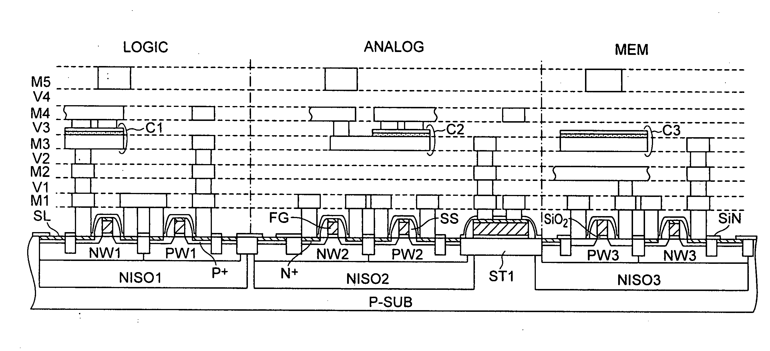
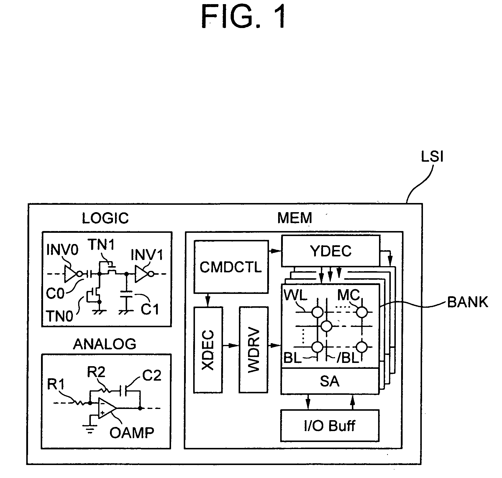
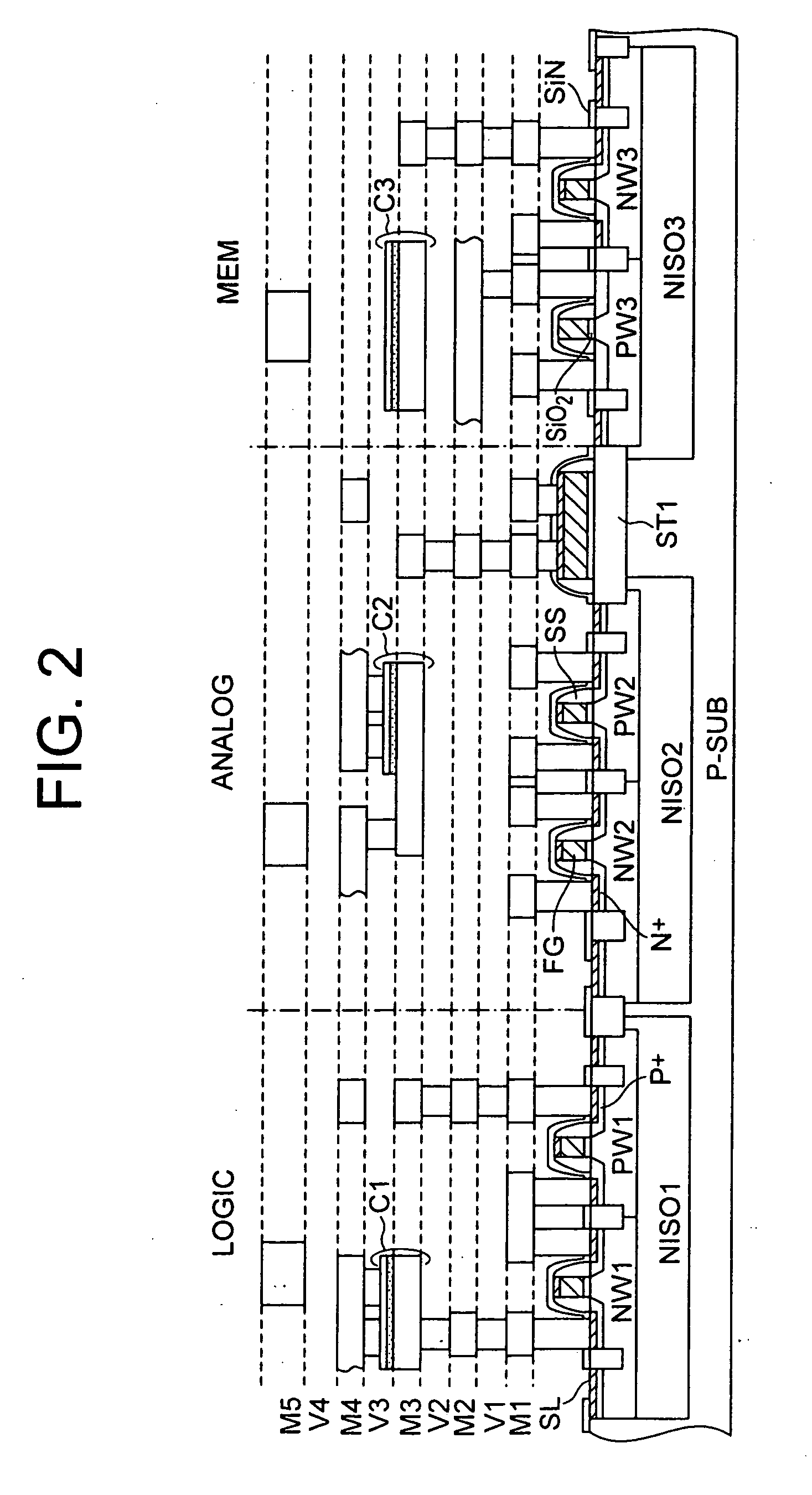
[0058]FIG. 1 is a diagram showing a semiconductor integrated circuit LSI (referred to as “LSI” hereinafter) which is one embodiment of the present invention. FIGS. 2 to 7 show practical embodiments of main parts making up the LSI of FIG. 1. FIG. 2 shows a cross-sectional diagram of a part of said LSI. FIG. 3 is an embodiment of a memory unit MEM which is the embodiment of FIG. 1; FIG. 4 is an embodiment of a memory cell MC in FIG. 3, which shows its circuit diagram and one example of operation waveforms. FIG. 5 shows a layout drawing of a 2T1C cell which was formed using a MIM capacitor. FIG. 6 is a diagram indicating the layout of the embodiment of FIG. 5 while classifying it in units of wiring layers. In addition, FIG. 7 is a diagram showing a cross-sectional structure of the 2T1C cell of FIG. 5. These embodiments will first be explained in the description below.

[0059]In the embodiment of FIG. 1, there is shown an embodiment of an LSI with a logic unit LOGIC, an analog unit ANALOG...

second embodiment

[0094]An explanation will be given of three modified examples of the memory cell layout of FIG. 4(a) of the first embodiment. In the memory cell layout shown in FIGS. 5 to 7, at the capacitor fabrication step, the dielectric film D0 is holed by etching process to thereby connect the wiring layer M3 and upper electrode P0 at an opening or hole of the dielectric film D0. At this time, the dielectric film D0 is exposed to a photolithography process resulting in unwanted contamination of the surface of dielectric film D0, which sometimes leads to a decrease in capacitor reliability and yield. In this case, a barrier metal may be used on or above the dielectric film D0 to thereby form capacitors. However, the use of such barrier metal would result in an unintentional increase in process cost. If this is the case, the use of a memory cell layout of FIG. 8, 9 and a fabrication method of FIG. 10 makes it possible to improve the capacitor reliability without using any barrier metal. A first ...

third embodiment

[0119]Although in the aforesaid embodiment the explanation was given while aiming at the memory cell made up of two transistors and one capacitor, an explanation will be given of the layout of a memory cell which is structured from two transistors and two capacitors in the next embodiment. In case no differences are found between one capacitor and two capacitors, handle them as a single carrier storage means. FIG. 18 depicts an arrangement with the memory cell MC in FIGS. 1 and 3 being modified to 2T2C. FIG. 18(a) is a circuit diagram, (b) shows operation waveforms during reading, and (c) shows operation waveforms during writing. The memory cell MC of this implementation is a 2T2C cell which consists essentially of two transistors TN1 and TN2 and two capacitors C0-C1. The drain of TN1 is connected to a bit line BL, and the source of TN1 is connected to one electrode of the capacitor C0 and then becomes a storage node SN1. Similarly the drain of TN2 is connected to a bit line / BL; th...


PUM


Abstract

A memory cell capacitor (C3) of a DRAM is formed by use of a MIM capacitor which uses as its electrode a metal wiring line of the same layer (M3) as metal wiring lines within a logic circuit (LOGIC), thereby enabling reduction of process costs. Higher integration is achievable by forming the capacitor using a high dielectric constant material and disposing it above a wiring layer in which bit lines (BL) are formed. In addition, using 2T cells makes it possible to provide a sufficient signal amount even when letting them operate with a low voltage. By commonizing the processes for fabricating capacitors in analog (ANALOG) and memory (MEM), it is possible to realize a semiconductor integrated circuit with the logic, analog and memory mounted together on one chip at low costs.

Description

[0001]The present application is a divisional application of application Ser. No. 10 / 488,401, filed Mar. 3, 2004, the contents of which are incorporated herein by reference.TECHNICAL FIELD[0002]The present invention relates to a semiconductor device and a manufacturing method thereof. In particular, the invention relates to a semiconductor device preferably adaptable for use in applications under high speed, high integration, and low power requirements.BACKGROUND ART[0003]The quest for higher functionality and higher performance is growing rapidly in a variety of types of information equipment including, but not limited to, mobile tools such as cellular phones, multimedia instruments such as game machines, personal computers or equivalents thereto. Under such circumstances, integrated circuits (referred to as LSI hereinafter) making up these apparatuses are more strictly required to offer higher performances in near feature, in terms of high integration, high-speed operability, low ...

Claims


Application Information

Patent Timeline
Patent Type & Authority Applications(United States)
IPC IPC(8): H01L27/108H01L23/522H01L27/10H10B12/00H10B69/00H10B99/00
CPCH01L23/5223H01L27/105H01L27/10814H01L27/10852H01L27/10885H01L27/10894H01L2924/0002H01L27/115H01L27/1052H01L2924/00H10B12/315H10B12/033H10B12/482H10B12/09H10B69/00
Inventor AKIYAMA, SATORUWATANABE, TAKAOMATSUI, YUICHIHIRATANI, MASAHIKO
Owner RENESAS ELECTRONICS CORP
Learn More