Integrated circuits with substrate protrusions, including (but not limited to) floating gate memories

Active Publication Date: 2008-10-30
PROMOS TECH INC
View PDF10 Cites 201 Cited by
  • Summary
  • Abstract
  • Description
  • Claims
  • Application Information

AI Technical Summary

Benefits of technology

[0011]In some embodiments of the present invention, the floating gate's top surface comes down along at least two sides of the protrusion to a level below the top of the protrusion. In some embodiments, the control gate's bottom surface als

Problems solved by technology

The current drive can be increased by reducing the thickness of tunnel oxide 120, but then data retention would be compromised as the charge leakage from the flo

Method used


Image

  • Integrated circuits with substrate protrusions, including (but not limited to) floating gate memories
  • Integrated circuits with substrate protrusions, including (but not limited to) floating gate memories
  • Integrated circuits with substrate protrusions, including (but not limited to) floating gate memories

Examples


Embodiment Construction

[0023]The embodiments described in this section illustrate but do not limit the invention. In particular, the invention is not limited to specific materials, circuits, dimensions, or other features or advantages except as defined by the appended claims.

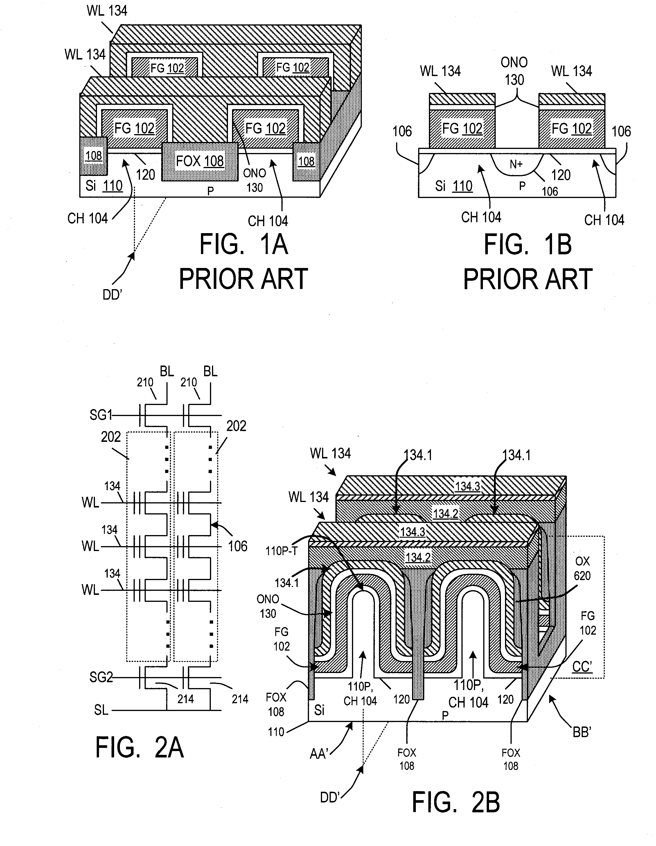
[0024]Some embodiments of the invention will now be described on the example of a NAND floating gate memory whose circuit diagram is shown in FIG. 2A. The memory includes a number of strings 202 of serially connected memory cells. The cells of each string 202 are connected in series between a respective select transistor 210 and a respective select transistor 214. The gate of transistor 210 is connected to a respective line SG1. The gate of transistor 214 is connected to a respective line SG2. The source of transistor 214 is connected to a respective source line SL. One line SG1, one line SG2, and one source line SL are shared by a number of memory strings 202 which form a memory block. Each transistor 210 connects the corresponding m...


PUM


Abstract

A floating gate memory cell's channel region (104) is at least partially located in a fin-like protrusion (110P) of a semiconductor substrate. The floating gate's top surface may come down along at least two sides of the protrusion to a level below the top (110P-T) of the protrusion. The control gate's bottom surface may also comes down to a level below the top of the protrusion. The floating gate's bottom surface may comes down to a level below the top of the protrusion by at least 50% of the protrusion's height. The dielectric (120) separating the floating gate from the protrusion can be at least as thick at the top of the protrusion as at a level (L2) which is below the top of the protrusion by at least 50% of the protrusion's height. A very narrow fin or other narrow feature in memory and non-memory integrated circuits can be formed by providing a first layer (320) and then forming spacers (330) from a second layer without photolithography on sidewalls of features made from the first layer. The narrow fin or other feature are then formed without further photolithography in areas between the adjacent spacers. More particularly, a third layer (340) is formed in these areas, and the first layer and the spacers are removed selectively to the third layer. The third layer is used as a mask to form the narrow features.

Description

CROSS REFERENCE TO RELATED APPLICATIONS[0001]The present application is a division of U.S. patent application Ser. No. 11 / 739,482 filed on Apr. 24, 2007, incorporated herein by reference.BACKGROUND OF THE INVENTION[0002]The present invention relates to integrated circuits having protrusions in a substrate. Examples of such integrated circuits include floating gate memories with substrate protrusions.[0003]FIG. 1A is a perspective view of a conventional NAND memory with floating gates 102. FIG. 1B shows a vertical cross section of the memory along a plane DD′ shown in FIG. 1A. Plane DD′ passes through channel regions 104 and source / drain regions 106. Floating gates 102 are conductive elements made from doped polysilicon. Substrate isolation regions 108 (“field oxide” or FOX) are formed in P-type silicon substrate 110. Silicon dioxide 120 (“tunnel oxide”) is formed on substrate 110 under the floating gates. ONO 130 (a sandwich of silicon oxide, silicon nitride, silicon oxide) insulate...

Claims


Application Information

Patent Timeline
IPC IPC(8): H01L29/788
CPCH01L27/115H01L27/11521H01L29/42324H01L29/7854H01L29/7881H10B69/00H10B41/30
Inventor HE, YUE-SONGMEI, LEN
Owner PROMOS TECH INC
Why Eureka
Try Eureka