Solid-state image capturing apparatus, method for manufacturing the same, and electronic information device

a technology of solid-state image and capturing apparatus, which is applied in the direction of color television, television system, radio control device, etc., can solve the problems of residual image degrading image quality, difficult to apply conventional reducing the resolution of solid-state image capturing apparatus, etc., to achieve the effect of improving light receiving efficiency, reducing readout voltage, and enlarge the size of the light receiving region

Active Publication Date: 2008-10-30
SHARP KK
View PDF0 Cites 32 Cited by
  • Summary
  • Abstract
  • Description
  • Claims
  • Application Information

AI Technical Summary

Benefits of technology

[0060]In addition, trench sections having a depth at least reaching light receiving sections are arranged adjacent to respective layers of the laminated light receiving sections in respective different substrate plane directions, and readout gate electrodes are embedded inside the trench sections to transfer signal charges from the light receiving sections. Each of the trenches adjacent to respective light receiving section is not adjacent to other light receiving sections, and therefore, readout voltage can be applied to the readout electrodes to read out signal charges corresponding to each color of the respective light receiving section independently from the light receiving section that is adjacent to that readout gate electrode (trench section). In addition, signal charges can be read out with low readout voltage because the readout gate electrode and the light receiving section are adjacent to each other. Further, because the trench sections are formed at the depths that reach from the substrate surface opposite from the light incident surface to the respective light receiving sections and the readout gate electrodes are not grounded on the substrate surface, it is possible to enlarge the size of the light receiving region to improve its light receiving efficiency.
[0061]As described above, it is possible to solve an issue that the location for a readout electrode for at least reading out signals need to be, not a narrow, but a wider trench, an issue that signal readout voltage increases due to a long distance between a readout electrode and a light receiving section or a channel, and an issue of a mixture of colors, the issue of a mixture of colors being solved by reading out signals of respective colors at independent locations and directions.
[0062]As described above, productivity for the solid-state image capturing apparatus can be increased because a step of forming a color filter as a manufacturing process related to an optical characteristic unique to the solid-state image capturing apparatus can be eliminated. In addition, because the light receiving sections for respective color signals can be formed by laminating them, a light receiving region of each of the pixel sections may be enlarged, leading to high image quality due to the improved light receiving sensitivity.
[0063]In addition, since the readout gate electrodes are formed inside the trench sections of the semiconductor substrate and read out in a vertical direction from the light receiving sections corresponding to respective colors, the readout gate electrodes and the light receiving sections are adjacent to each other; and because the distances between the readout gate electrodes and the channel sections are short, signal charges can be read out by much lower readout voltage, thereby reducing power consumption. Further, since it is not needed to form a high concentration diffusion layer as a transfer path or to provide a readout gate electrode on the substrate surface, an establishment area can be smaller and a size of a light receiving region in each pixel section can be substantially larger, leading to high image quality due to the improved light receiving sensitivity.
[0064]Further, since wiring layers are provided on the opposite side surface from the light incident surface, it is not needed to arrange wiring layers in between pixel sections, the wiring layers for transferring signal charges outputted from each pixel section (each light receiving section). Therefore, establishment areas for wiring layers will not cause the solid-state image capturing apparatus to lower its resolution. Further, it is possible to form a transistor on the opposite side from the light incident surface, the transistor being necessary for amplifying signal charges and electrical resetting of signal charges from the light receiving sections. Because the area of the light receiving region of each pixel section is not affected by an area for arranging the transistor, it will not cause the solid-state image capturing apparatus to lower its resolution, and the area of the light receiving region can be larger, leading to high image quality due to the improved light receiving sensitivity. In addition, note that a signal readout circuit and its wiring may be provided on the light incident side (between the light receiving sections; and between adjacent solid-state image capturing devices, for example). In this case, a depth of a trench can be shallow, thereby making the manufacturing easier.
[0065]Therefore, according to the present invention, the solid-state image capturing apparatus with high sensitivity and high resolution, which needs no color filter that is needed for a conventional solid-state image capturing apparatus and is capable of reading out signal charges corresponding to a plurality of colors separately with low voltage, can be realized with a simple manufacturing method with a step of forming a color filter eliminated. Further, an electronic information device using the solid-state image capturing apparatus as an image input device for an image capturing section thereof can also be realized.

Problems solved by technology

However, each of the conventional solid-state image capturing apparatuses described above has the following problems.
This results in a reduction of a resolution of the solid-state image capturing apparatus due to the area taken for arranging the high concentration diffusion layer and readout gate electrode.
Therefore, it is difficult to apply the conventional solid-state image capturing apparatus disclosed in Reference 1 directly for a CMOS image sensor used for low electricity consumption purpose.
If read out is performed with a low voltage used for a CMOS image sensor, signal charges will not be read out completely and they will be left in a light receiving section, leading to defect of causing a residual image to degrade an image quality.
In this case, since light receiving sections for respective colors are arranged on the same surface, it is difficult to enlarge a size of a light receiving region in each pixel section, and its light receiving sensitivity decreases as the area of the light receiving region is downsized.
Further, with this structure, since a color filter needs to be provided and therefore use efficiency for incident light decreases for the amount of the light absorbed by the color filter, a problem of decreasing of light receiving sensitivity occurs.

Method used


Image

  • Solid-state image capturing apparatus, method for manufacturing the same, and electronic information device
  • Solid-state image capturing apparatus, method for manufacturing the same, and electronic information device
  • Solid-state image capturing apparatus, method for manufacturing the same, and electronic information device

Examples


embodiment 1

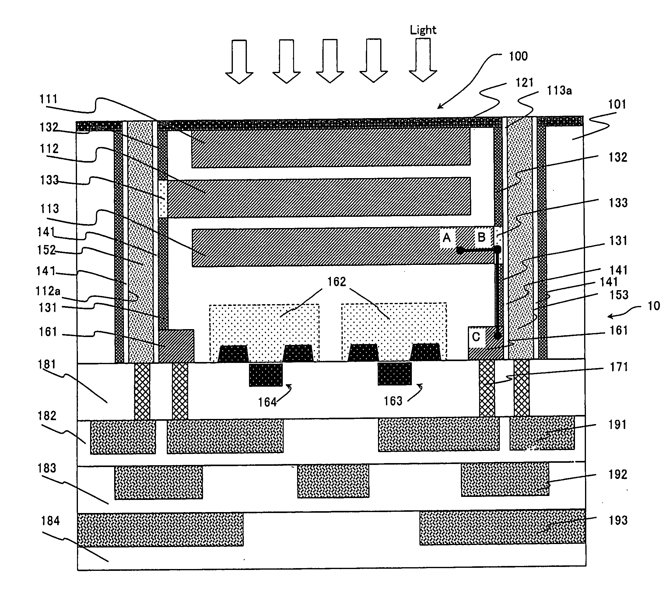
[0107]FIG. 1 is a longitudinal cross-sectional view showing an exemplary essential structure of a solid-state image capturing device according to Embodiment 1 of the present invention.

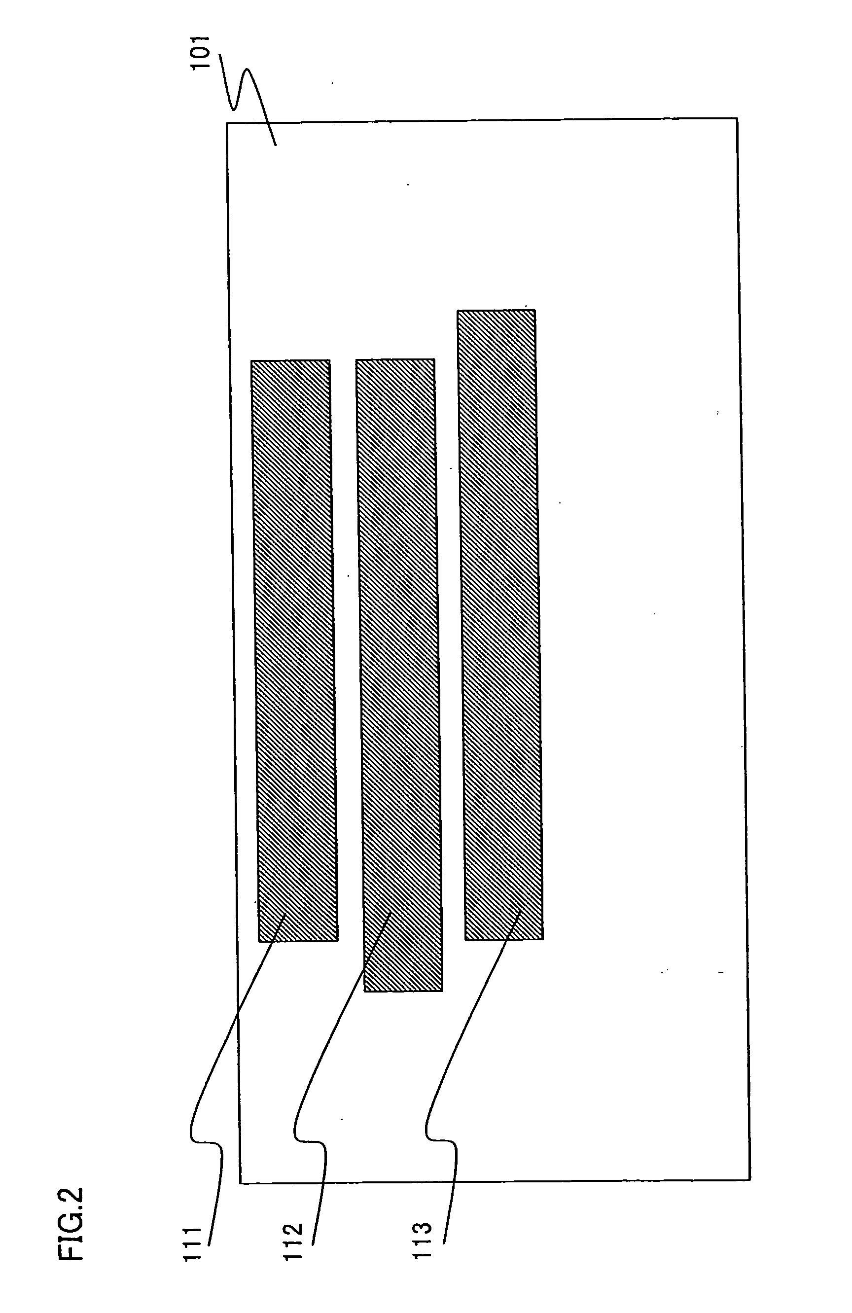
[0108]In a solid-state image capturing device 100 according to Embodiment 1 in FIG. 1, a case is described where the solid-state image capturing device 100 includes a first light receiving section 111 for detecting an electromagnetic wave of a first wavelength band, a second light receiving section 112 for detecting an electromagnetic wave of a second wavelength band, and a third light receiving section 113 for detecting an electromagnetic wave of a third wavelength band, as a plurality of light receiving section. In this case, three colors having different wavelength bands of light are considered to be, for example, three primary colors of R (red), G (green), and B (blue). Hereinafter, a case is described where blue light is detected in the first wavelength band, green light in the second wavelength b...

embodiment 2

[0144]In Embodiment 1 described above as shown in FIG. 3(A), where the light receiving sections 111-113 are arranged in a square or rectangle lattice shape, the three layered light receiving sections 111-113 each are formed such that respective sides of the light receiving sections are extended towards different substrate plane directions from the center (the sides of the light receiving sections are extended towards the periphery in such a way that the light receiving sections each will not overlap in a plane view). In Embodiment 2, as shown in FIG. 3(B), a case is described where each of the pixel sections is arranged in a hexagon shape in a plane view and the plurality of the pixel sections are arranged in a honeycomb structure (beehive structure), in which each of the pixel sections is shifted by a half period in the honeycomb structure, and three layers of the light receiving sections 211-213 are formed in such a way that each of the edges of the respective light receiving sect...

embodiment 3

[0148]In Embodiment 1 described above, the solid-state image capturing device 10 laminated with three layers of the light receiving sections 111-113 to detect three primary colors of R, G and B. In Embodiment 3, a case is described where a solid-state image capturing apparatus has a solid-state image capturing device, whose light receiving sections are laminated with four layers to detect four colors.

[0149]In Embodiment 3, there are N (N is a natural number) numbers of light receiving sections provided in a depth direction of a semiconductor substrate, the light receiving sections being from the first light receiving section for detecting an electromagnetic wave of a first wavelength band to the Nth light receiving section for detecting an electromagnetic wave of an Nth wavelength band. A case is provided here where the plural number of Nth layers is four layers. In such a case as this, four layers (four colors) of light receiving sections, such as a first light receiving section fo...


PUM


Abstract

An image capturing apparatus has a plurality of solid-state image capturing devices each having light receiving sections laminated in a depth direction of a semiconductor substrate. The devices are sequentially arranged in a direction along a substrate surface. Incident light waves having wavelength bands corresponding to depths of respective light receiving sections are detected there and generate signal charges. Bands are associated with light receiving sections by the wavelength dependence of the optical absorption. Trench sections each reach from a light incident surface or an opposite substrate surface to respective light receiving sections that do not overlap each other in a plane view. Electric charge transfer sections transfer electric charges independently from the light receiving sections via side wall portions of their respective trenches to the light incident surface side or the opposite substrate surface side at the time of driving readout gate electrodes at each trench section.

Description

[0001]This Nonprovisional application claims priority under 35 U.S.C. §119(a) on Patent Application No. 2007-097461 filed in Japan on Apr. 3, 2007, the entire contents of which are hereby incorporated by reference.BACKGROUND OF THE INVENTION[0002]1. Field of the Invention[0003]The present invention relates to a solid-state image capturing apparatus (e.g., a CMOS image sensor, a CCD image sensor and the like) where lights with different wavelengths are separated and detected by a plurality of light receiving sections laminated in a depth direction of a semiconductor substrate or a semiconductor layer, a method for manufacturing the solid-state image capturing device, and an electronic information device (e.g., a digital camera, a cell phone device equipped with a camera and the like) using the solid-state image capturing apparatus as an image input device for an image capturing section thereof.[0004]2. Description of the Related Art[0005]In a conventional color solid-state image capt...

Claims


Application Information

Patent Timeline
Patent Type & Authority Applications(United States)
IPC IPC(8): H01L23/00H01L21/00H01L27/146H01L27/148H04N5/335H04N5/359H04N5/369H04N5/372H04N5/374
CPCH01L27/14636H01L27/14645H04N23/10H04N23/12
Inventor AKIYOSHI, MUTOH
Owner SHARP KK
Why Eureka
Try Eureka