Plasma display panel and method for producing the same

a technology of display panel and plasma, which is applied in the manufacture of electrode systems, electric discharge tubes/lamps, discharge tubes luminescnet screens, etc., can solve the problems of insufficient cure of the lower layer to be removed during development, high manufacturing cost, and inability to meet the requirements of a single layer, so as to achieve stable production of display panels, reduce manufacturing costs, and reduce manufacturing costs

Inactive Publication Date: 2008-11-06
PANASONIC CORP
View PDF12 Cites 6 Cited by
  • Summary
  • Abstract
  • Description
  • Claims
  • Application Information

AI Technical Summary

Benefits of technology

[0032]In this display panel, the projected amounts of both the end portions of the bus electrode having the two-layered structure are small, in other words, the flexure of the white layer is small. Accordingly, the yield of this display panel is high, and the display panel can be stably produced. Also, in this display panel, failure in insulation and pressure proof is hard to occur, since thickness of a dielectric layer which covers the display panel is not locally decreased or a local thinning is decreased.
[0033]According to the production method of the present invention, a portion at which an electrode pattern is to be formed is exposed by applying light, while a part of the surface of such a portion is shielded from light, and such a portion is then developed to form the electrode pattern, so that it becomes possible to form a recess on the surface of the electrode after the development. As a result, the thermal shrinkage of the center portion and the thermal shrinkage of the end portions of the electrode in the widthwise direction during the calcining step can be controlled separately. Therefore, it is possible to form the electrode in which the flexure of its white layer and the projection of the end portions thereof in the widthwise direction of the electrode are suppressed. Therefore, according to this production method, it is possible to provide a PDP having high performance for insulation and pressure proof.

Problems solved by technology

Consequently, the amount of the insufficiently cured lower layer to be removed during development becomes larger than that of the upper layer.
As a result, failures in insulation and pressure proof are more likely to occur, and the manufacturing yield becomes lower, which results in higher manufacturing cost.
Under such a situation, there is a problem that a production has not yet been realized wherein a bus electrode by a decreased number of steps, that is, by collectively exposing and developing two layers for the bus electrode, while preventing failures in insulation and pressure proof in the electrode.

Method used


Image

  • Plasma display panel and method for producing the same
  • Plasma display panel and method for producing the same
  • Plasma display panel and method for producing the same

Examples


example 1

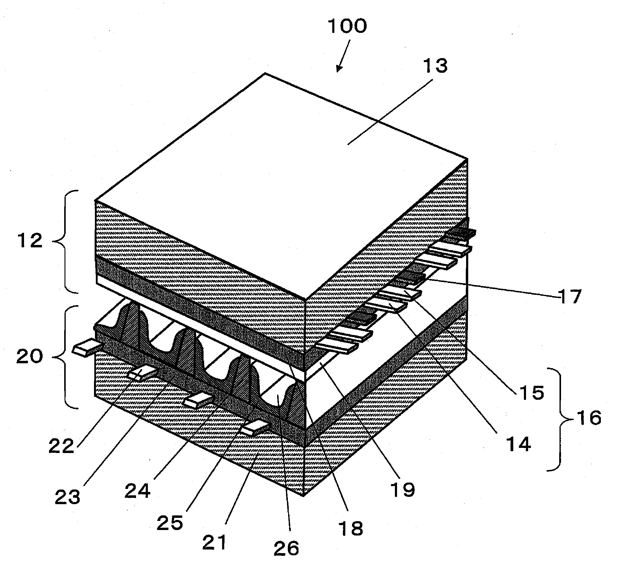
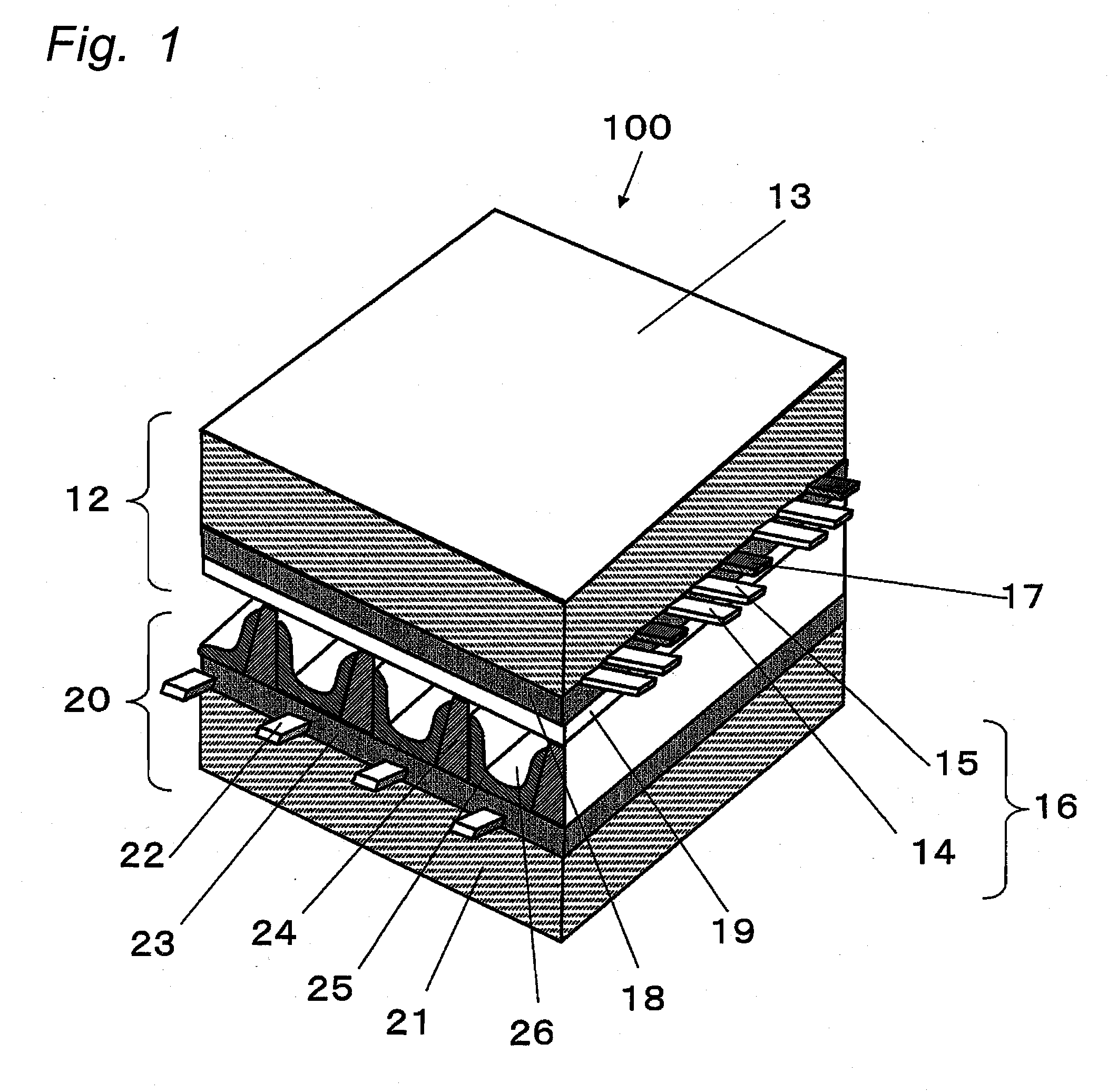
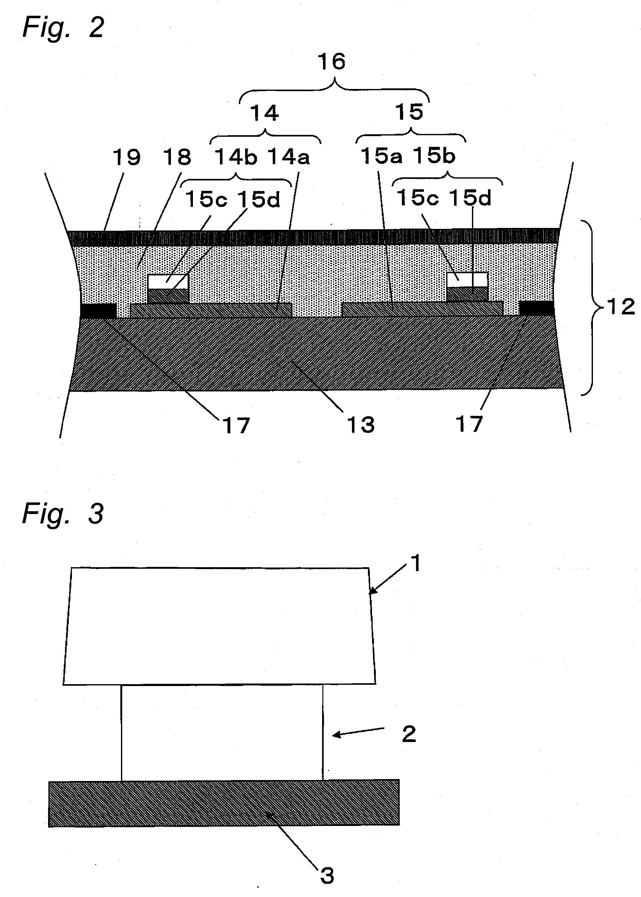
[0159]In Example 1, the width W of the electrode shown in FIG. 7(c) was 120 μm. The exposure was carried out while the distance L from the end portion of the light-shielding member in the widthwise direction of the electrode pattern was changed within a range of 0.5 to 18 μm, and while the width T of the light-shielding member in the widthwise direction of the electrode was changed within a range of 1 to 14 μm; and the electrode pattern was developed. After that, the electrodes were calcined at 600° C. to form the bus electrodes 14b and 15b. One hundred samples were fabricated for each one combination of T and L.

[0160]Next, a paste of a dielectric material was applied by the die coating method, to cover the bus electrodes 14b and 15b, and was dried at 100° C. and calcined at 600° C. to form a dielectric layer with a thickness of 50 μm. The dielectric material paste was prepared by mixing a glass frit which contained bismuth oxide (Bi2O3), boron oxide (B2O3) and silicon oxide (SiO2) ...

example 2

[0164]Electrodes were fabricated in the same manner as in Example 1, except that the width W of the electrode shown in FIG. 7(c) was set at 40 μm.


PUM


Abstract

A method for producing a plasma display panel wherein the projection of the end portions of electrode in the widthwise direction are suppressed so that failure in insulation and pressure proof is not caused upon forming an electrode pattern by collectively exposing and developing a bus electrode having a two-layered structure. When the electrode pattern having two-layered structure by a photolithography method using a mask, exposure is made by applying light, while a part of a surface of portion of a paste film of an electrode material which portion to be formed into the electrode pattern is shield from the light, so that a dent is formed in the electrode surface after developing and the thermal shrinkage of the center portion and the thermal shrinkage of the end portions of the electrode in the widthwise direction are controlled separately by the dent.

Description

BACKGROUND OF THE INVENTION[0001]The present invention relates to a plasma display panel and a method for producing a plasma display panel. In particular, the present invention pertains to a plasma display panel characterized by the surface configurations of the electrodes on its front panel, and a method for producing a plasma display panel.[0002]A plasma display panel (hereinafter referred to as PDP) has a structure comprising a front panel and a back panel arranged facing each other, which are sealed at their peripheral portions; and discharge gases such as neon (Ne), xenon (Xe) and the like are sealed in a discharge space defined between the front panel and the back panel.[0003]The front panel is provided with a plurality of display electrodes each consisting of a scan electrode and a sustain electrode forming stripes, which are formed on one surface of a glass substrate, and a dielectric layer and a protective layer which cover these display electrodes. Each of the display elec...

Claims


Application Information

Patent Timeline
Patent Type & Authority Applications(United States)
IPC IPC(8): H01J1/62H01J9/00H01J17/49H01J9/02H01J11/12H01J11/22H01J11/24H01J11/26H01J11/34
CPCH01J9/02H01J11/12H01J11/24H01J11/22
Inventor HORIKAWA, AKIHIRONAGINO, TOSHIFUMI
Owner PANASONIC CORP
Why Eureka
Try Eureka