Thin film device with lead conductor film of increased surface area

a lead conductor film and thin film technology, applied in the direction of recording information storage, instruments, transportation and packaging, etc., can solve the problems of increasing loss and heat generation, difficult to efficiently radiate heat, and increasing the volume of thin film devices, so as to reduce loss and heat generation

Active Publication Date: 2008-11-06
TDK CORPARATION
View PDF10 Cites 0 Cited by
  • Summary
  • Abstract
  • Description
  • Claims
  • Application Information

AI Technical Summary

Benefits of technology

[0006]It is an object of the present invention to provide a high frequency thin-film device capable of reducing loss and heat generation due to skin effect, parti...

Problems solved by technology

In thin-film devices of this type, since the signal frequency has been increased for higher speed and performance, the ensuing increase in loss and heat generation due to the skin effect that a signal current flows at the surface of a lead conductor film in a concentrated manner has become a problem.
In thin-film devices of this type, however, there is generally adopted a structure in which a thin-film element and a lead conductor film are embedded in an insulating film, and such a structure requires a system through which heat generated at the lead conductor film by th...

Method used


Image

  • Thin film device with lead conductor film of increased surface area
  • Thin film device with lead conductor film of increased surface area
  • Thin film device with lead conductor film of increased surface area

Examples


Embodiment Construction

1. Thin-Film Device

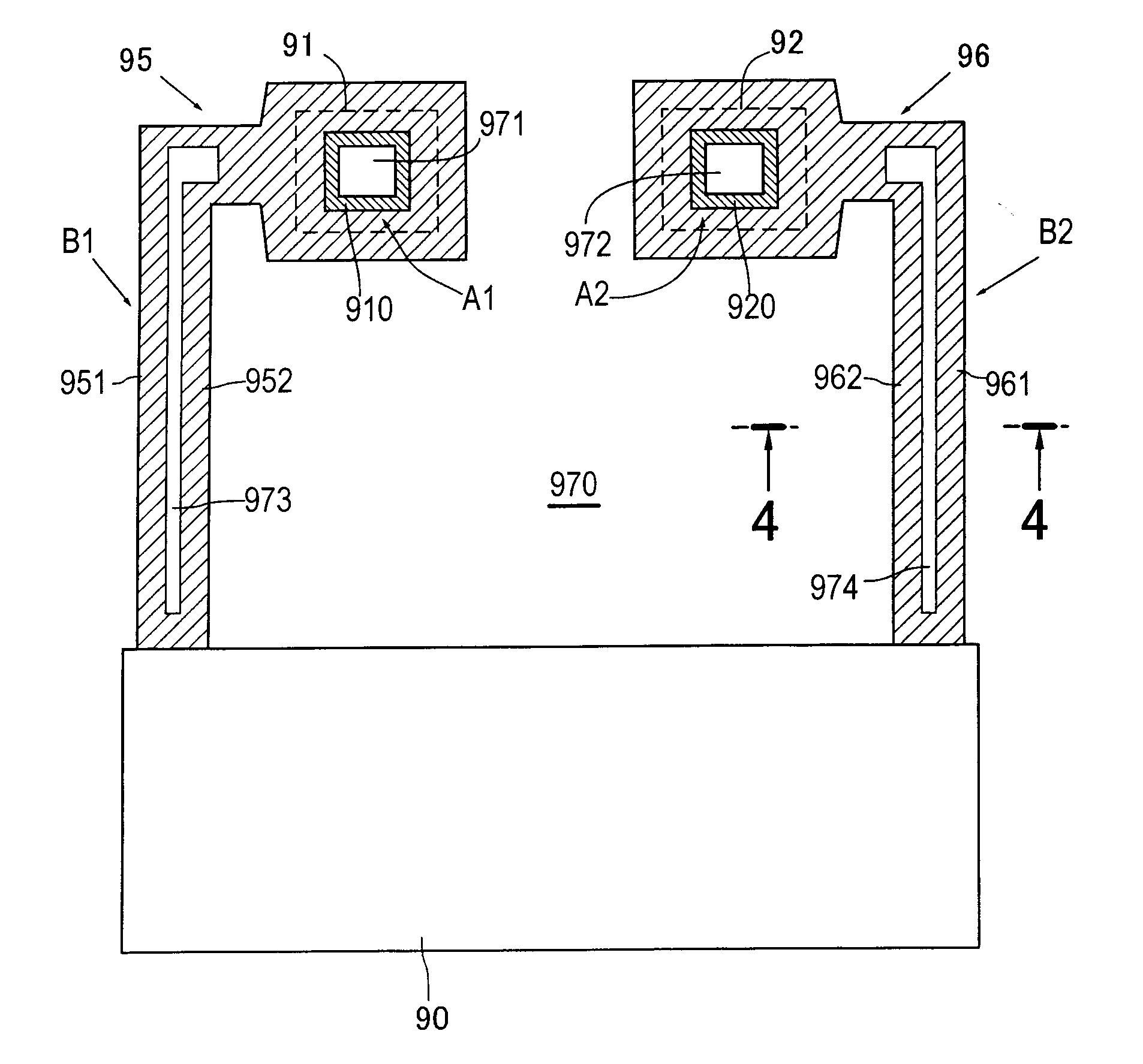
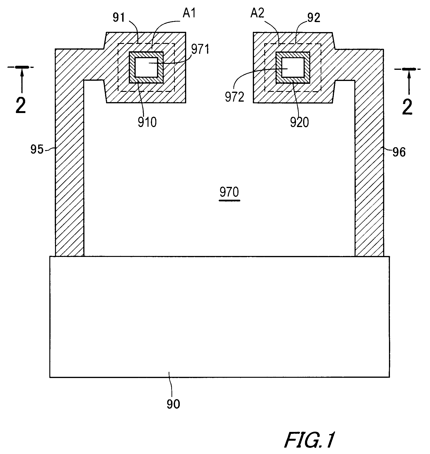
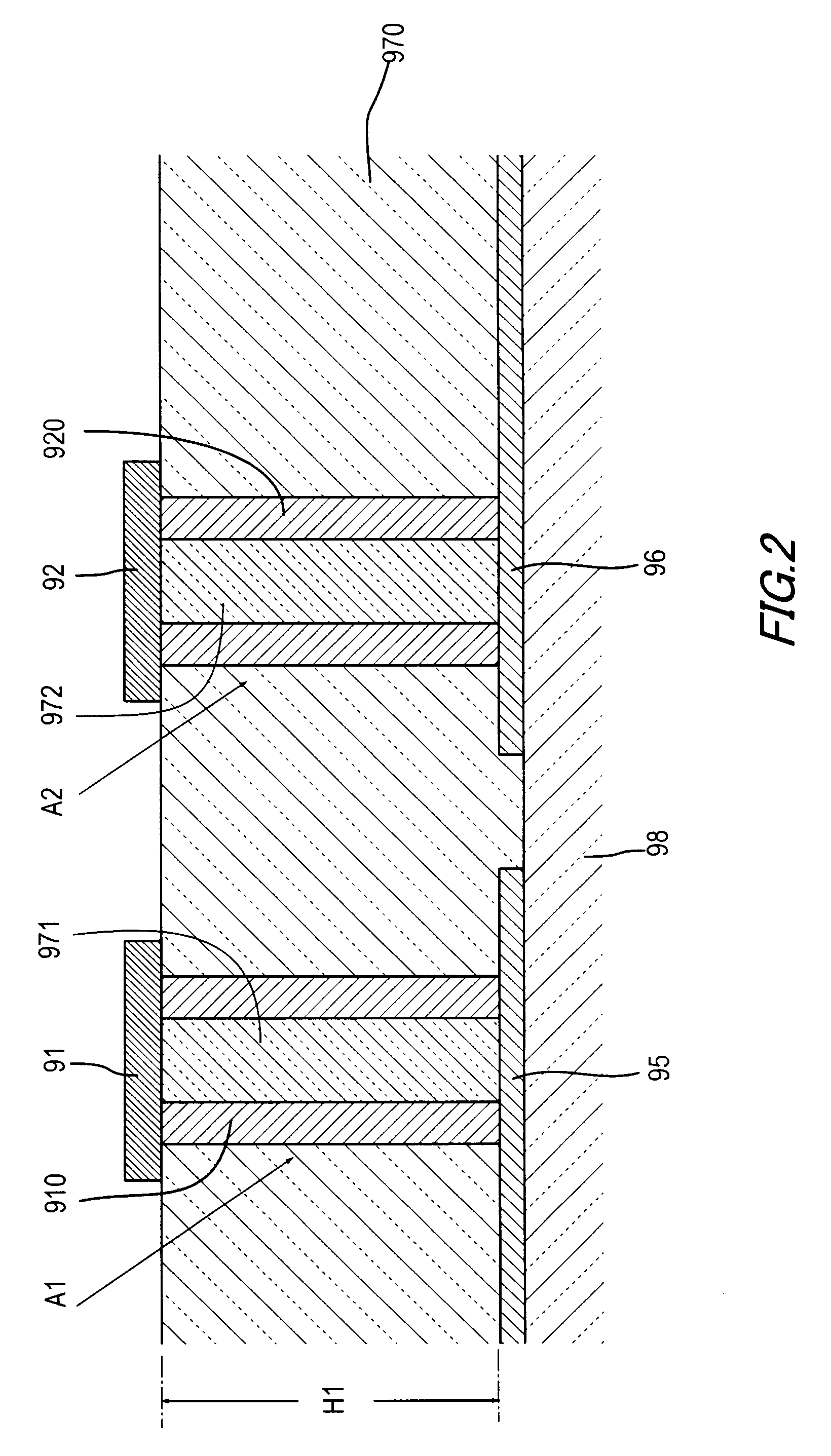
[0043]A thin-film device illustrated in FIGS. 1 and 2 includes a thin-film element 90, a lead conductor film (95, 910), a lead conductor film (96, 920), and bumps 91, 92.

[0044]The thin-film element 90 is in the form of a thin-film and at least one selected from an electromagnetic conversion element, a passive element and an active element. More specifically, examples include a MR element, a recording element, a memory element for use in a MRAM (magnetoresistive random access memory), a magnetic sensor element, a coil element, a resistive element, and a capacitor element. They may be used alone or in combination with each other. The thin-film magnetic head is a typical example of a case where a MR element is combined with a coil element. The MR element may include a SV film or a TMR film. The thin-film device according to the present invention may be an assembly of an array of thin-film elements 90 or may be an individual body.

[0045]The lead conductor film (95, 910...


PUM


Abstract

The present invention relates to a thin-film device including a thin-film element and a lead conductor film. The thin-film element and the lead conductor film are embedded in an insulating film. The lead conductor film has a terminal area at one end thereof, is connected to the thin-film element at the other end thereof, and between the one end and the other end, has an increased surface area portion whose volume is partially occupied by an insulating material to increase surface area. As a result, there is provided a high frequency thin-film device capable of reducing loss and heat generation due to skin effect, particularly a thin-film magnetic head.

Description

TECHNICAL FIELD[0001]The present invention relates to a thin-film device, a thin-film magnetic head, a head assembly and a magnetic recording / reproducing apparatus.BACKGROUND OF THE INVENTION[0002]Thin-film devices covered by the present invention include a magneto-resistive effect element (hereinafter referred to as “MR element”), a variety of semiconductor elements and a circuit element such as an inductor. Among them, the MR element is used not only as a magnetic detecting element or a magnetic memory but also as a reproducing element for a thin-film magnetic head. The inductor forms an independent circuit element by itself and is also used as a recording element for a thin-film magnetic head.[0003]In thin-film devices of this type, since the signal frequency has been increased for higher speed and performance, the ensuing increase in loss and heat generation due to the skin effect that a signal current flows at the surface of a lead conductor film in a concentrated manner has be...

Claims


Application Information

Patent Timeline
IPC IPC(8): G11B5/39G11B5/127G11B5/64
CPCY10T428/1121G11B5/4853
Inventor MIYATA, SHINGOYAMAGUCHI, ATSUSHINOGUCHI, KIYOSHISATO, MAKOTO
Owner TDK CORPARATION
Why Eureka
Try Eureka