Conductive Thin Film and Thin Film Transistor

Inactive Publication Date: 2008-11-13
PANASONIC CORP
View PDF2 Cites 39 Cited by
  • Summary
  • Abstract
  • Description
  • Claims
  • Application Information

AI Technical Summary

Benefits of technology

[0093]The present invention, which is practiced by the above-described solution means, is capable of providing an inexpensive and flexible conductive thin film having excellent carrier mobility and electric conductivity which is formed by highly orienting nanotube or an electronic functional organic material by simple and convenient means, as well as a thin film transistor employing such a conductive film.
[0094]According to the embodiment wherein the conductive thin film is formed by using the composite-type material comprising a mixture of nanotube and the liquid crystalline organic compound, since the nanotube is highly oriented by utilizing a high degree of orientation of the liquid crystalline organic compound, the conductive thin film having excellent carrier mobility and electric conductivity and the thin film transistor employing the conductive thin film can be fabricated by a simple and convenient method.
[0095]According to the embodiment wherein the conductive thin film is formed from the liquid crystalline electronic functional organic material comprising the non-liquid-crystalline electronic functional organic material and the non-liquid-crystalline organic compound which are hydrogen-bonded to each other, since the liquid crystalline electronic functional organic material is highly oriented by utilizing the conventional orientation technique, the conductive thin film having excellent carrier mobility and electric conductivity and the thin film transistor employing the conductive thin film can be fabricated by a simple and convenient method.
[0096]According to the embodiment wherein the aforementioned liquid crystalline electroni

Problems solved by technology

Thus, such a conductor or semiconductor layer comprising an electronic functional organic material has a problem that the carrier mobility thereof is considerably lower than that of a layer comprising an inorganic semiconductor.
The carrier mobility of the conductor or semiconductor layer comprising an electronic functional organic material is considerably lower than that of the layer comprising an inorganic semiconductor because the conductor or semiconductor layer formed by mere evaporation or deposition of the electronic functional organic material has electronic functional organic material molecules therein wit

Method used


Image

  • Conductive Thin Film and Thin Film Transistor
  • Conductive Thin Film and Thin Film Transistor
  • Conductive Thin Film and Thin Film Transistor

Examples


Example

Embodiment 1

[0169]Embodiments 1 to 3 of the present invention to be described below are embodiments each realizing a conductive thin film which is further improved in electric conductivity and carrier mobility and which is formed by preparing a composite-type material by mixing carbon nanotube as a conductor or semiconductor material and a liquid crystalline organic compound together and aligning molecules of the carbon nanotube favorably and densely by utilizing favorable orientation of the liquid crystalline organic compound of the composite-type material, as well as a thin film transistor employing such a conductive thin film.

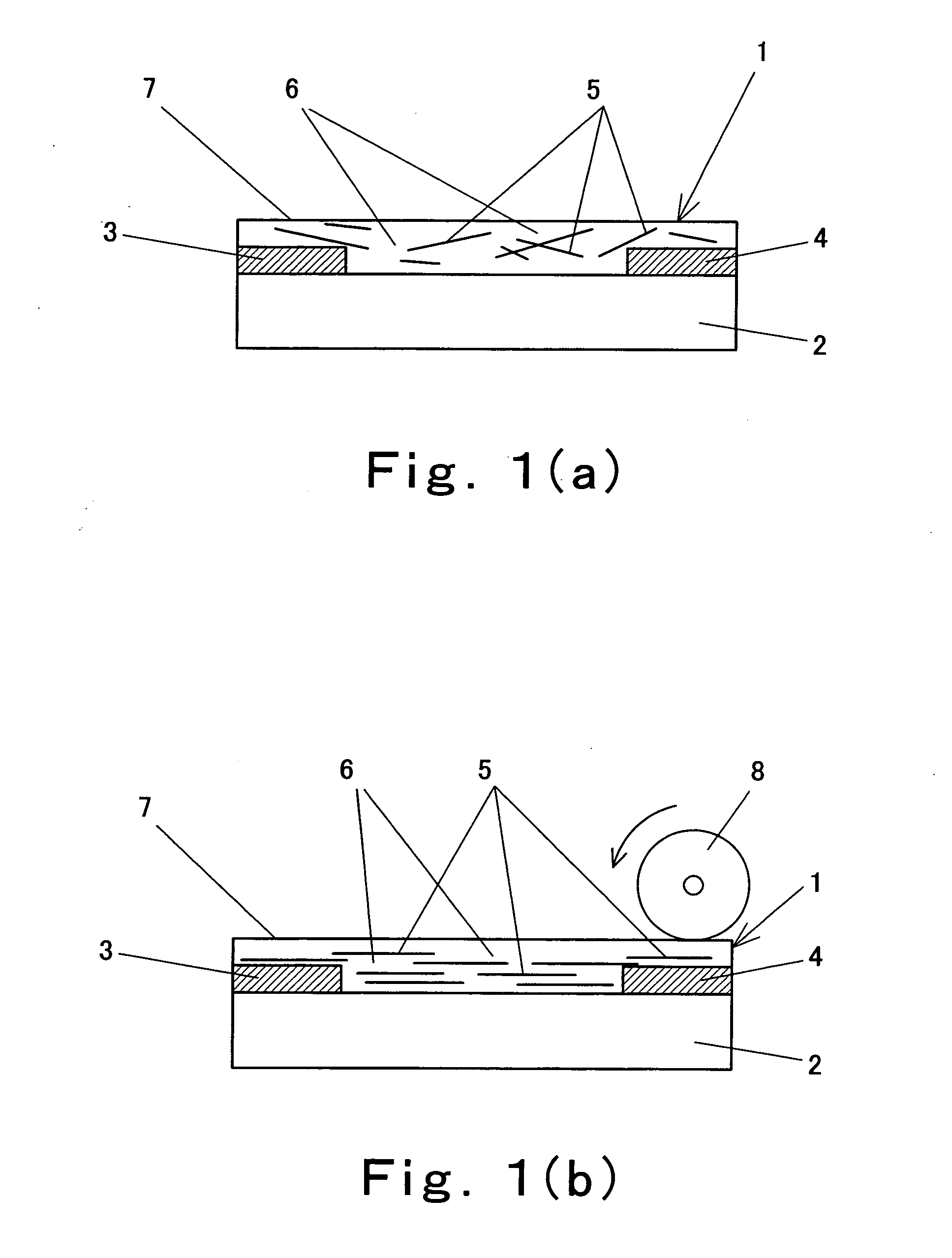
[0170]FIG. 1 is a sectional view schematically illustrating a part of a process for forming a conductive thin film according to embodiment 1 of the present invention.

[0171]The conductive thin film 1 shown in FIG. 1 is formed in the following manner. In FIG. 1(a), two electrodes 3 and 4 of such a material as gold are disposed opposite to each other across a s...

Example

Embodiment 2

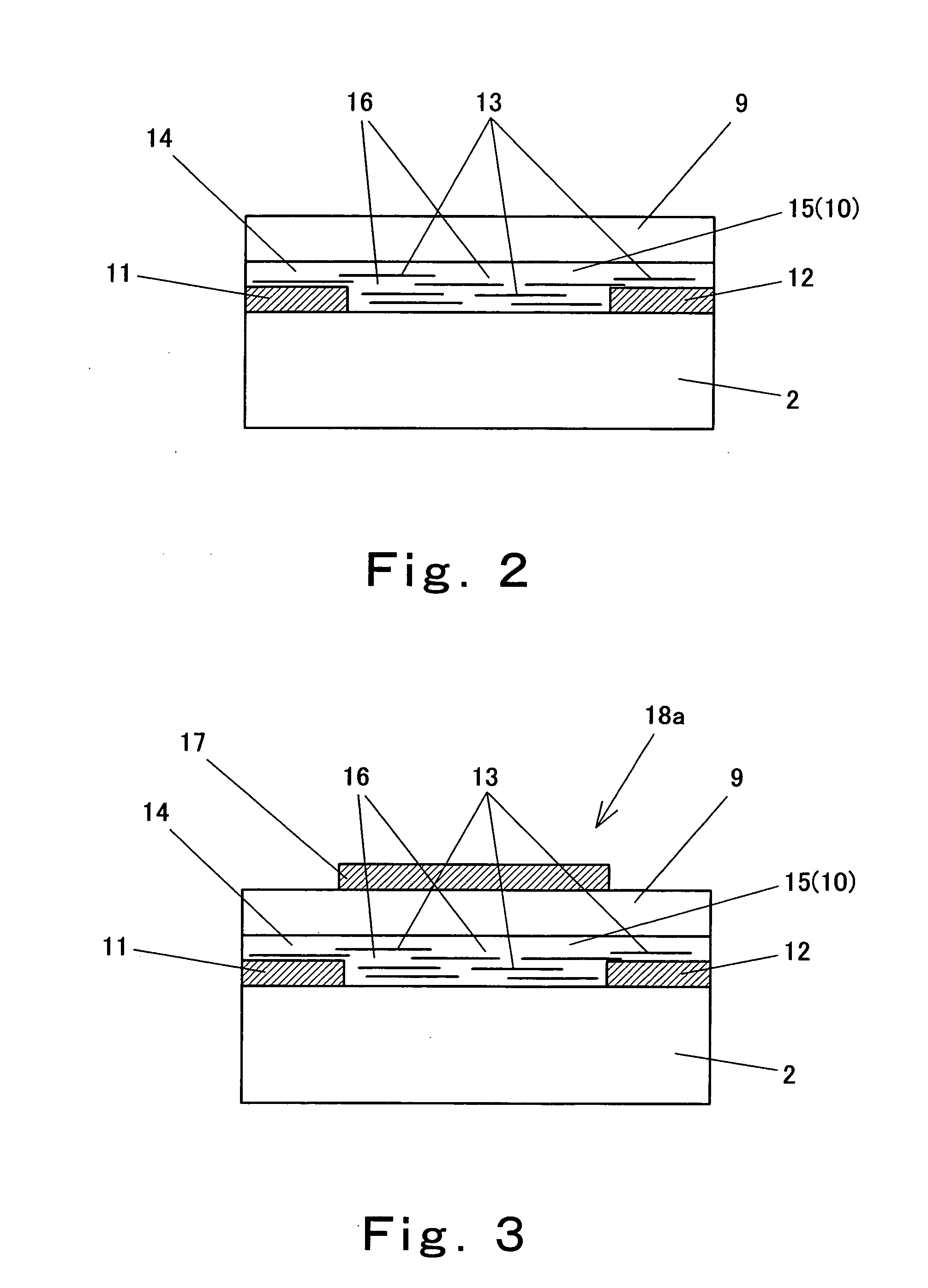
[0181]FIG. 2 is a sectional view schematically illustrating a part of a process for forming a composite-type semiconductor layer in which a conductive thin film according to embodiment 2 of the present invention is used as a semiconductor layer.

[0182]The composite-type semiconductor layer 15 as the semiconductor layer 10 in FIG. 2 is formed in the following manner. An orientation film (not shown), such as a polyimide film or a monomolecular film, is formed over a surface of a region in which at least a channel (not shown) is to be formed so as to cover at least a part of each of source and drain electrodes 11 and 12 disposed opposite to each other on a substrate 2 and an upper surface of the substrate 2 lying in the space intervening between these electrodes. The orientation film is then oriented in a predetermined direction by such orientation means as rubbing. Thereafter, a composite-type compound 14 prepared by mixing semiconductive carbon nanotube 13 and a liquid cry...

Example

Embodiment 3

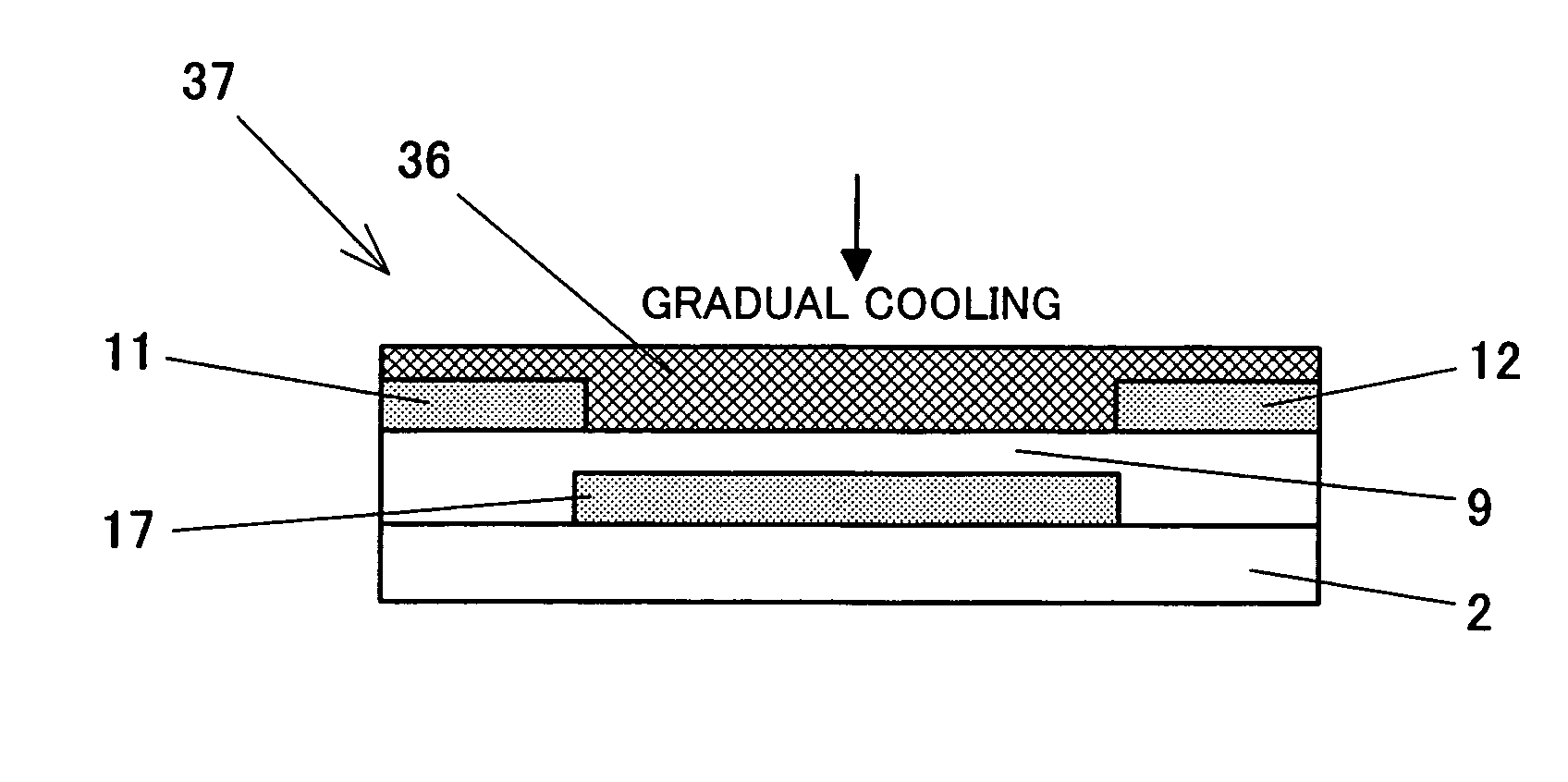
[0188]FIG. 3 is a sectional view schematically showing the construction of a thin film transistor according to embodiment 3 of the present invention.

[0189]As shown in FIG. 3, the thin film transistor 18a according to the present embodiment has source and drain electrodes 11 and 12 formed on a substrate 2 by patterning such an electrode material as gold. The thin film transistor 18a also has a composite-type semiconductor layer 15 formed as semiconductor layer 10 by a method to be described later, the composite-type semiconductor layer 15 being interposed between the source and drain electrodes 11 and 12 and a gate insulator 9 to be described later. Over an upper surface of the composite-type semiconductor layer 15 is formed the gate insulator 9 comprising silicon oxide, a polyvinylidene fluoride organic compound or the like. The thin film transistor 18a further has a gate electrode 17 formed of such an electrode material as gold on the upper side of the gate insulator 9....


PUM


Abstract

[Object] To provide an inexpensive and flexible conductive thin film which is excellent in carrier mobility and electric conductivity and which is formed by highly orienting nanotube or an electronic functional organic material by simple and convenient means, as well as a thin film transistor using the conductive thin film.
[Solution Means] A conductive thin film (1) is formed by mixing a first material (5) having electric conductivity or semiconductivity and a second material (6) to prepare a mixture and orienting the mixture by utilizing liquid crystallinity thereof.

Description

TECHNICAL FIELD[0001]The present invention relates to a conductive thin film formed by orienting nanotube or an organic semiconductor compound as well as a thin film transistor employing the same as a semiconductor layer.BACKGROUND ART[0002]A thin film transistor (TFT) for use in flat panel displays and the like has a structure wherein source and drain electrodes are disposed on one side of a semiconductor layer forming part of the thin film transistor and a gate electrode disposed on the other side of the semiconductor layer at a substantially central position relative to a channel.[0003]Usually, a semiconductor layer of a thin film transistor having the above-described structure is formed by processing a semiconductor thin film formed on a substrate under precise control based on a thin film control process. Here, the semiconductor layer of the thin film transistor formed by the thin film control process calls for an excellent carrier mobility for a semiconductor device to be cons...

Claims


Application Information

Patent Timeline
IPC IPC(8): H01L51/00H01B1/24H01L29/78H01L51/30H01L51/40
CPCB82Y10/00H01L51/0012H01L51/0048H01L51/0052H01L51/0055H01L51/0068H01L51/0072H01L51/0076H01L51/0541H10K71/191H10K85/221H10K85/623H10K85/655H10K85/731H10K85/615H10K85/6572H10K10/464
Inventor WAKITA, NAOHIDE
Owner PANASONIC CORP
Why Eureka
Try Eureka