Semiconductor light emitting device

a technology of light-emitting devices and semiconductors, which is applied in the direction of semiconductor devices, basic electric elements, electrical equipment, etc., can solve the problems of insufficient light-emitting efficiency, achieve the effects of reducing the positional separation between electrons and holes, improving light-emitting efficiency, and reducing the number of transistors

Inactive Publication Date: 2008-11-20
SUMITOMO ELECTRIC DEVICE INNOVATIONS
View PDF0 Cites 20 Cited by
  • Summary
  • Abstract
  • Description
  • Claims
  • Application Information

AI Technical Summary

Benefits of technology

[0010]The present invention has been made in view of the above circumstances and improves the light-emitting efficiency.
[0011]According to an aspect of the present invention, there is provided a semiconductor light emitting device including a substrate and a quantum well active layer. The quantum well active layer has a plurality of barrier layers made of GaN-based semiconductor and a well layer made of GaN-based semiconductor sandwiched between the barrier layers and has polarized charge between the barrier layer and the well layer caused by piezo polarization. The well layer has a composition modulation so that a band gap is minimum at an interface between the well layer and one of the barrier layers more far from the substrate than the other. With the structure, positional separation between an electron and a hole is restrained. And light-emitting efficiency is improved.

Problems solved by technology

However, the light-emitting efficiency is not sufficient even if the MQW active layer disclosed in Document 1 is used.

Method used


Image

  • Semiconductor light emitting device
  • Semiconductor light emitting device
  • Semiconductor light emitting device

Examples


first embodiment

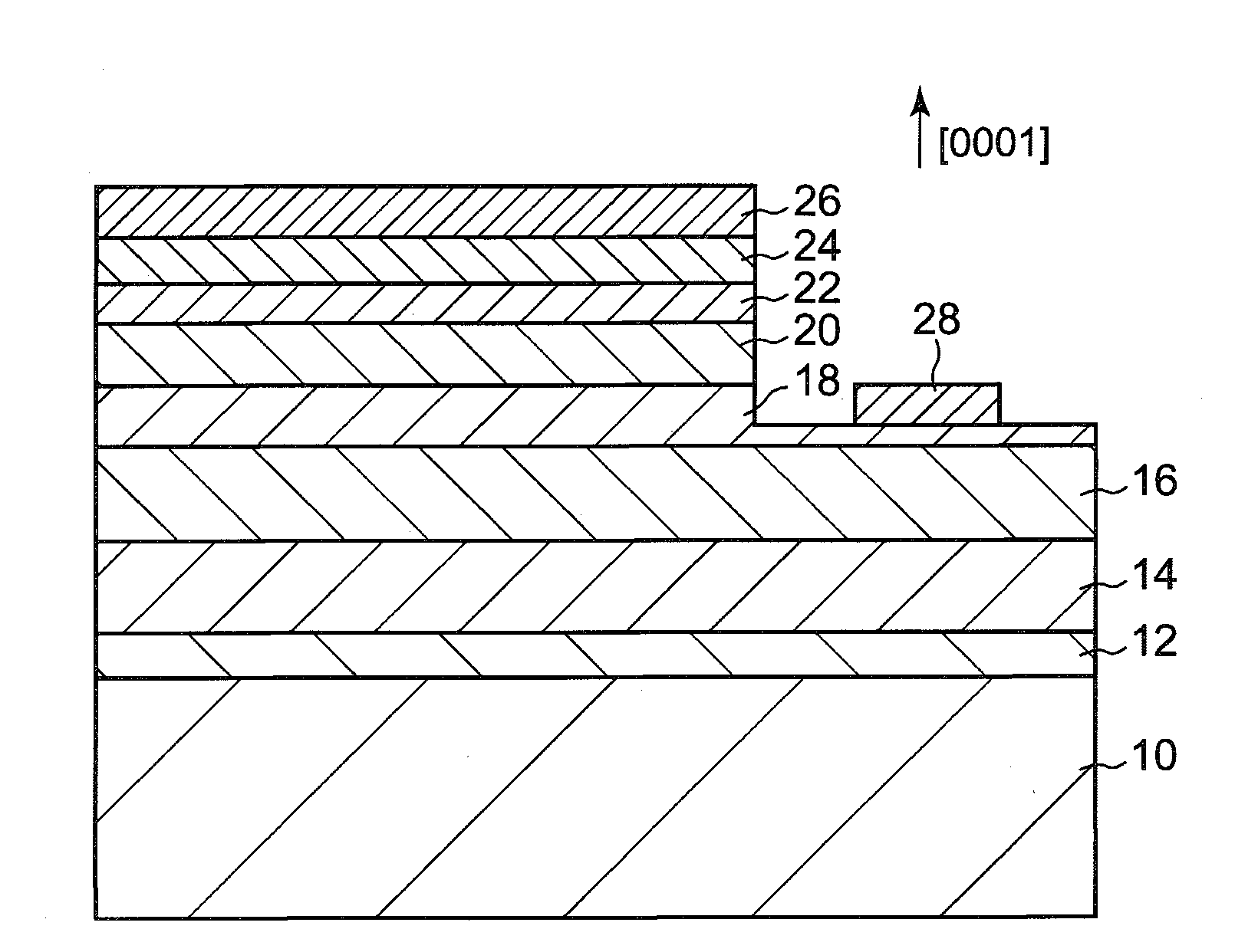
[0026]FIG. 4 illustrates a cross section view of a LED in accordance with a first embodiment. As shown in FIG. 4, there are laminated an AlN buffer layer 12, a GaN buffer layer 14, an N-type first GaN cladding layer 16, an N-type InGaN contact layer 18, an N-type second GaN cladding layer 20 (corresponding to a first conductivity type semiconductor layer), a MQW active layer 22 and a P-type GaN cladding layer 24 (corresponding to a second conductivity type semiconductor layer) on a sapphire substrate 10 in order, with MOCVD method. Each layer is formed so that a normal line direction of the substrate 10 is [0001]. A P electrode 26 is formed on the P-type GaN cladding layer 24. An N electrode 28 is formed on the N-type InGaN contact layer 18.

[0027]A growth condition of each layer is given below.

[0028]The AlN buffer layer 12 at high temperature: thickness was 0.1 μm; undoped; growth temperature was 1230 degrees C.; and carrier gas was hydrogen.

[0029]The GaN buffer layer 14: thickness ...

second embodiment

[0050]FIG. 9 illustrates a case where the contact layer is not used. As shown in FIG. 9, a semiconductor light emitting device in accordance with a second embodiment has a Si-doped N-type GaN cladding layer 16a (corresponding to the first conductivity type semiconductor layer) having thickness of 2 μm instead of the N-type first GaN cladding layer 16, the N-type InGaN contact layer 18 and the N-type second GaN cladding layer 20, being different from FIG. 5 of the first embodiment. The N electrode 28 is electrically connected to the N-type GaN cladding layer 16a. The other structure is the same as that of the first embodiment shown in FIG. 5.

[0051]The AlN buffer layer 12 grown at high temperature has crystal quality and the a-axis lattice constant of the GaN layer grown on the AlN buffer layer 12 is reduced because of the AlN buffer layer 12, in a case where the high-temperature AlN buffer layer 12 is used as in the case of the first embodiment and the second embodiment. Therefore, i...

third embodiment

[0053]A third embodiment shows a case where a low-temperature GaN buffer layer is used. As shown in FIG. 10, a low-temperature GaN buffer layer 12a is used instead of the high-temperature AlN buffer layer 12 of the first embodiment shown in FIG. 5. The growth condition of the low-temperature GaN buffer layer 12a is shown below.

[0054]The low-temperature GaN buffer layer 12a: thickness is 0.1 μm; undoped; growth temperature is 600 degrees C.; and carrier gas is hydrogen.

[0055]A Si-doped N-type GaN cladding layer 16b (corresponding to the first conductivity type semiconductor layer) having thickness of 5 μm is used instead of the GaN buffer layer 14, the N-type first GaN cladding layer 16, the N-type InGaN contact layer 18 and the N-type second GaN cladding layer 20. The other structure is the same as that of FIG. 5 in the first embodiment. The low-temperature buffer layer may be used as in the case of the third embodiment.


PUM


Abstract

A semiconductor light emitting device includes a substrate and a quantum well active layer. The quantum well active layer has a plurality of barrier layers made of GaN-based semiconductor and a well layer made of GaN-based semiconductor sandwiched between the barrier layers and has polarized charge between the barrier layer and the well layer caused by piezo polarization. The well layer has a composition modulation so that a band gap is minimum at an interface between the well layer and one of the barrier layers more far from the substrate than the other.

Description

BACKGROUND OF THE INVENTION[0001]1. Field of the Invention[0002]The present invention relates a semiconductor light emitting device, and in particular, relates to a semiconductor light emitting device having a quantum well active layer.[0003]2. Description of the Related Art[0004]A semiconductor light emitting device such as LED (Light Emitting Diode) or LD (Laser Diode) having a GaN (gallium nitride)-based semiconductor is being used as a light emitting device for short wavelength.[0005]Japanese Patent Application Publication No. 2005-056973 (hereinafter referred to as Document 1) discloses a semiconductor light emitting device having a MQW (Multi Quantum Well) active layer made of GaN-based semiconductor. As shown in FIG. 5 of Document 1, an N-type cladding layer, a MQW active layer, and a P-type cladding layer are laminated on a substrate. FIG. 1A through FIG. 2B illustrate In composition ratio and energy of a well layer 30 and a barrier layer 32 of the semiconductor light emitti...

Claims


Application Information

Patent Timeline
Patent Type & Authority Applications(United States)
IPC IPC(8): H01L33/00H01L33/06H01L33/32
CPCH01L33/06H01L33/32
Inventor YUI, KEIICHI
Owner SUMITOMO ELECTRIC DEVICE INNOVATIONS
Why Eureka
Try Eureka