Display device and electronic device using thin-film transistors formed on semiconductor thin films which are crystallized on insulating substrates

a technology of semiconductor thin films and electronic devices, which is applied in semiconductor devices, solid-state devices, antenna supports/mountings, etc., can solve the problems of restricted mounting of components in the device, unsuitable conventional display devices,

Inactive Publication Date: 2008-11-20
SHARP KK
View PDF3 Cites 6 Cited by
  • Summary
  • Abstract
  • Description
  • Claims
  • Application Information

AI Technical Summary

Benefits of technology

[0018]It was understood that in the thin-film transistor provided on the insulating substrate, high-frequency characteristics of GHz or more can be obtained by using a semiconductor thin film that is crystallized in a predetermined direction, and by setting the direction of carriers flowing in the thin-film transistor to accord with the direction of crystallization. Therefore, the formation of an amplifier circuit, etc. for analog signals in a region of GHz or more was made easier.

Problems solved by technology

However, the conventional display device is not suited to the ubiquitous society which is expected to come in the future and realize “anytime, anywhere” networking.
As regards an electronic device, such as a mobile phone, which needs to be reduced in size, there is a problem that the mounting of components in the device is restricted by a flexible cable that is connected to the display.

Method used


Image

  • Display device and electronic device using thin-film transistors formed on semiconductor thin films which are crystallized on insulating substrates
  • Display device and electronic device using thin-film transistors formed on semiconductor thin films which are crystallized on insulating substrates
  • Display device and electronic device using thin-film transistors formed on semiconductor thin films which are crystallized on insulating substrates

Examples


Embodiment Construction

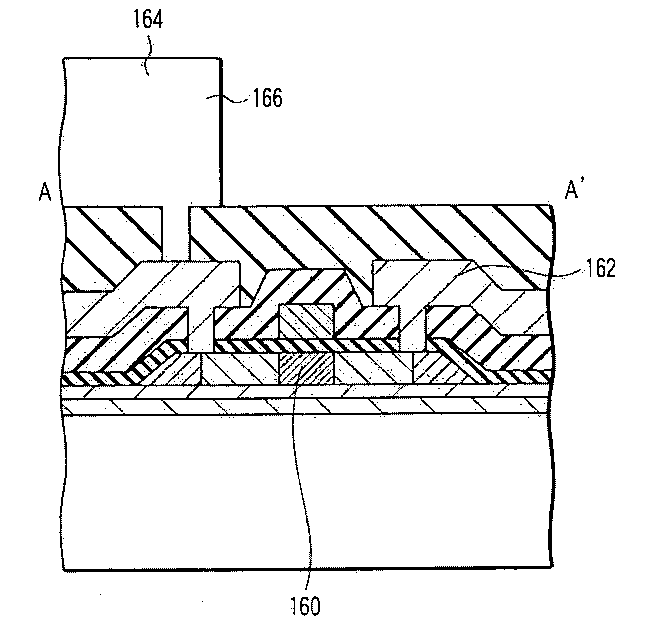
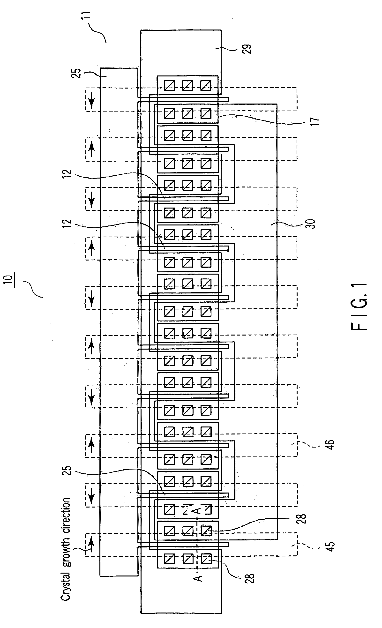
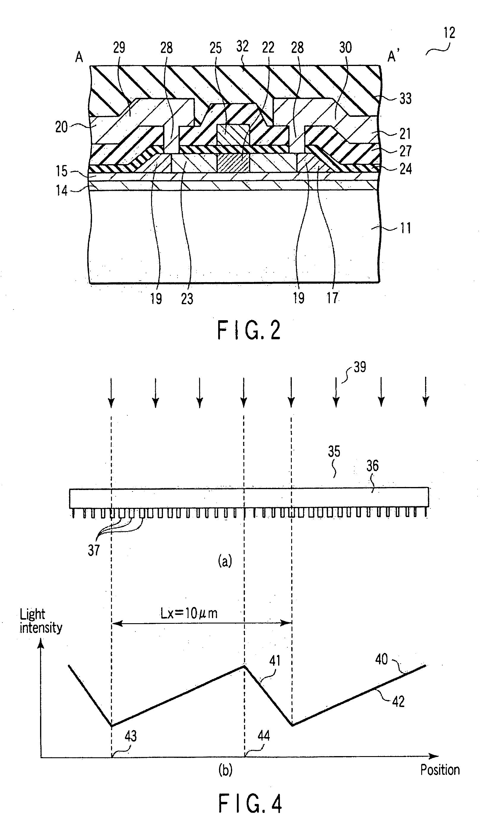
[0045]To begin with, a thin-film transistor, which is used in the present invention, is described. FIG. 1 is a plan view of a thin-film transistor circuit 10 with a channel width of 200 microns. In the thin-film transistor circuit 10, ten field-effect thin-film transistors 12 each having a channel width of 20 microns are connected in parallel. The field-effect thin-film transistors 12 are formed on a semiconductor thin film which is recrystallized in a predetermined direction and is formed on an insulating substrate 11 that is a glass substrate in the present embodiment. The insulating substrate 11 is not limited to the glass substrate, and a quarts substrate or a plastic substrate may be used. In a transistor device which drives a large current, good characteristics can be maintained by disposing a plurality of transistors each having a small channel width in parallel. In addition, with this structure, thermal destruction due to self-heat-production of the device at the time of ope...


PUM


Abstract

A method of receiving video data, a control signal, etc. via a non-contact transmission path is adopted, and a receiving circuit for receiving and amplifying a signal is formed on the same insulating substrate as a display device. Thus, there are provided a thin-film transistor which is formed in a semiconductor thin film that is formed on the insulating substrate and crystallized in a predetermined direction, and an inductor for forming an inductive-coupling circuit, which is formed by using an electrically conductive thin film provided on the insulating substrate. The direction of movement of carriers flowing in the thin-film transistor is parallel to the direction of crystallization of the semiconductor thin film, and the inductor and the thin-film transistor are integrated so as to be electrically coupled directly or indirectly.

Description

CROSS-REFERENCE TO RELATED APPLICATIONS[0001]This application is based upon and claims the benefit of priority from prior Japanese Patent Applications No. 2007-130923, filed May 16, 2007; and No. 2008-098605, filed Apr. 4, 2008, the entire contents of both of which are incorporated herein by reference.BACKGROUND OF THE INVENTION[0002]1. Field of the Invention[0003]The present invention relates to a thin-film transistor formed on a semiconductor thin film which is deposited on an insulating substrate and is crystallized in a predetermined direction, and to an electronic device and a display device which are fabricated by using the thin-film transistors. In particular, the invention relates to an electronic device and a display device, which employ thin-film transistors having channel regions formed in regions that are crystal-grown in a lateral direction, and which are suitably applied to analog circuits which perform signal processing of 1 GHz or more.[0004]2. Description of the Rel...

Claims


Application Information

Patent Timeline
Patent Type & Authority Applications(United States)
IPC IPC(8): H01L33/00
CPCH01L27/12H01L27/13H01L27/1285H01L29/78696H01L29/04
Inventor KAWACHI, GENSHIRO
Owner SHARP KK
Why Eureka
Try Eureka