Method for preparing novel material layer structure of circuit board and article thereof

a technology of layer structure and circuit board, applied in the field of circuit boards, can solve the problems of serious high-frequency transmission loss of pi soft board, poor structural characteristics, and difficulty in meeting the requirements of 5g technology products, and achieve the effect of improving the performance of existing circuit board and reducing the cost of production

Pending Publication Date: 2022-08-25
LI LONGKAI
View PDF0 Cites 0 Cited by
  • Summary
  • Abstract
  • Description
  • Claims
  • Application Information

AI Technical Summary

Problems solved by technology

However, due to the larger dielectric constant and loss factor, higher moisture absorption and poor reliability of PI substrate, the high-frequency transmission loss of PI soft board is serious and its structural characteristics are poor, which cannot adapt to the current high-frequency and high-speed trend.
Therefore, with the emergence of new 5G technology products, the signal transmission frequency and speed of existing circuit boards have been difficult to meet the requirements of 5G technology products.
Meanwhile, in the preparation technique, there are many problems in the traditional multi-layer flexible circuit board or multilayer combination of hard and soft boards, such as more process flows, complex manufacturing process, and higher power consumption and signal transmission loss in circuit board performance.
During the use of the device, there will be a risk that the circuit will burn and explode due to the conductive collision between the lines, resulting in that the lines on the circuit board cannot work safely and normally.

Method used


Image

  • Method for preparing novel material layer structure of circuit board and article thereof
  • Method for preparing novel material layer structure of circuit board and article thereof

Examples


embodiment 1

[0036]This embodiment provides a method for preparing a novel material layer structure of a circuit board, comprising the steps of:

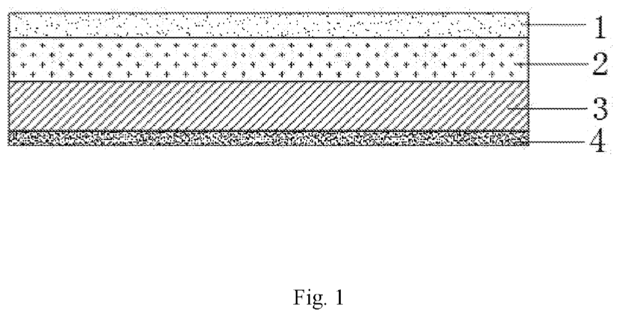
[0037](1) combining a film with a copper layer to form an FCCL single-sided board;

[0038](2) placing the FCCL single-sided board in a film covering machine, and applying a semi-cured functional material layer on the back of the film at a temperature of 60° C.-500° C., wherein the semi-cured functional material layer is an MPI film, an LCP film, a TFP film, a PTFE film, a copper ion migration resistant film, an LDK high-frequency functional adhesive, a copper ion migration resistant adhesive, or a mixture of the LDK high-frequency functional adhesive and the copper ion migration resistant adhesive to form a novel material layer structure for a circuit board.

[0039]In the step (2), a front surface and a back surface of the semi-cured functional material layer are provided with a release paper or a PET release film, respectively; and the release paper or the ...

embodiment 2

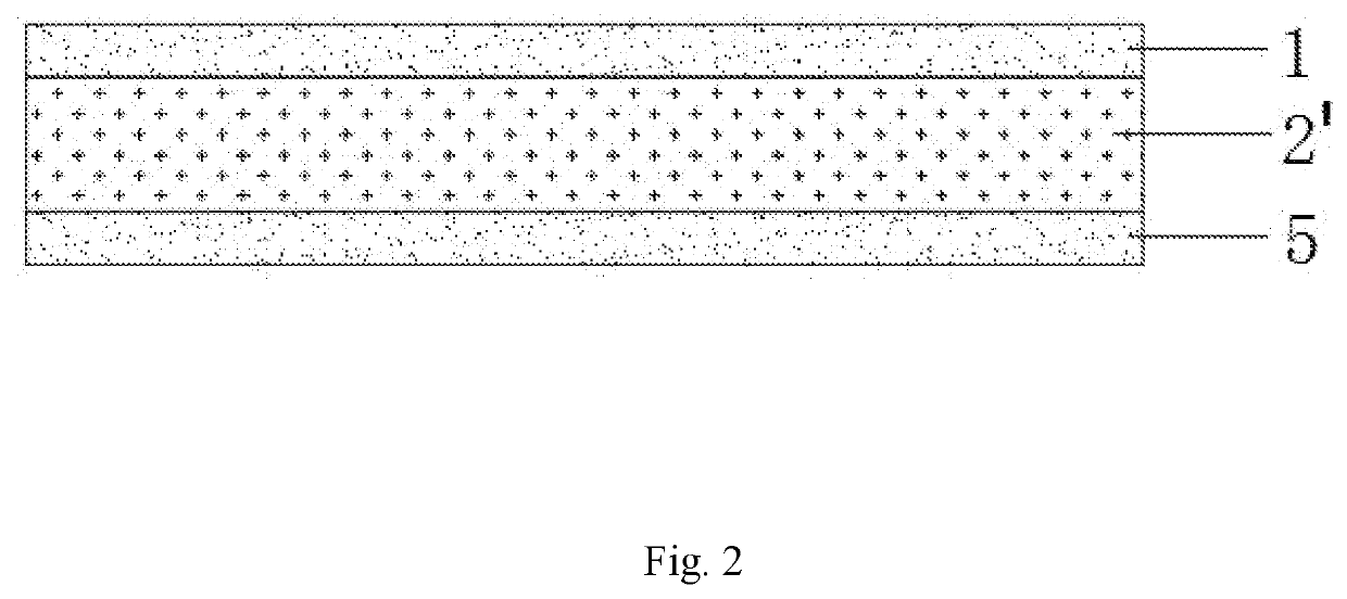
[0097]The main differences between this embodiment and embodiment 1 are as follows. It further comprises step (3) of tearing off the release paper or the PET release film on the back side of the semi-cured functional material layer, and hot-pressing a copper foil on the back surface of the semi-cured functional material layer to form a novel double-sided material layer structure of a circuit board.

[0098]Meanwhile, the semi-cured functional material layer described in this embodiment is any one of an MPI film, an LCP film, a TFP film, and a PTFE film. Furthermore, the semi-cured functional material layer and the film are of the same material. For example, the film and the semi-cured functional material layer are both an MPI film; the film and the semi-cured functional material layer are both an LCP film; the film and the semi-cured functional material layer are both a TFP film; or the film and the semi-cured functional material layer are both a PTFE film.

[0099]Therefore, a double-sid...


PUM

PropertyMeasurementUnit
temperatureaaaaaaaaaa
communication frequencyaaaaaaaaaa

Abstract

The present invention discloses a method for preparing a novel material layer structure of a circuit board, comprising the steps of: (1) combining a film with a copper layer to form an FCCL single-sided board; (2) applying a semi-cured functional material layer on a back side of the film of the FCCL single-sided board, wherein the semi-cured functional material layer is an MPI film, an LCP film, a TFP film, a PTFE film, a copper ion migration resistant film, an LDK high-frequency functional adhesive, a copper ion migration resistant adhesive, or a mixture of the LDK high-frequency functional adhesive and the copper ion migration resistant adhesive to form a novel material layer structure for a circuit board. An article prepared by performing the above methods is also disclosed. The prepared novel material layer structure of the circuit board has high-frequency characteristics and/or copper ion migration resistance, and can be used as an integral structure. In the circuit board manufacturing process, it can be manufactured as the circuit board manufacturing material to be different circuit board structures, which brings great convenience for subsequent circuit board manufacturing and simplifies the manufacturing process.

Description

TECHNICAL FIELD[0001]The present invention relates to the field of circuit boards, and more particularly, to a method for preparing a novel material layer structure of a circuit board and an article thereof.BACKGROUND ART[0002]At present, the communication frequency is overall high-frequency from the communication network to the terminal application. High-speed and large-capacity applications emerge endlessly. As wireless networks transition from 4G to 5G in recent years, network frequencies continue to rise. According to the 5G development roadmap shown in the relevant data, the future communication frequency will be promoted in two stages. The first phase aims to increase the communication frequency to 6 GHz by 2020, and the second phase to further increase it to 30-60 GHz by 2020. In the market application, the signal frequency of terminal antennas such as smart phones is increasing.There are more and more high-frequency applications, which acqure more and more demand for high-sp...

Claims


Application Information

Patent Timeline
Patent Type & Authority Applications(United States)
IPC IPC(8): H05K3/00H05K1/05
CPCH05K3/0011H05K1/056H05K2203/1581H05K2201/0141H05K2201/0145H05K2201/0154H05K2201/015H05K2201/0129H05K2201/0112B32B15/20B32B27/322B32B27/34B32B27/36B32B27/281B32B27/06B32B7/06B32B15/08B32B29/002B32B33/00B29D7/01B29C63/02B29C63/0065B29C65/02H05K3/022B32B2457/08
Inventor LI, LONGKAI
Owner LI LONGKAI
Why Eureka
Try Eureka