

Electronic component and manufacturing method therefor
a manufacturing method and technology of electronic components, applied in the field of electronic components, can solve the problems of large loss of high frequency characteristics and poor linearity of the edges and achieve the effects of improving high frequency characteristics, high frequency characteristics, and improving linearity of the edge portion of the planar electrod
- Summary
- Abstract
- Description
- Claims
- Application Information
AI Technical Summary
Benefits of technology
Problems solved by technology
Method used
Image

Examples
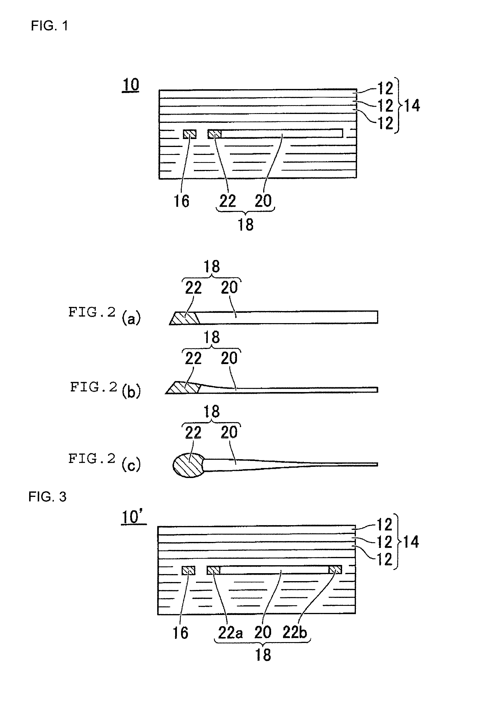
first embodiment
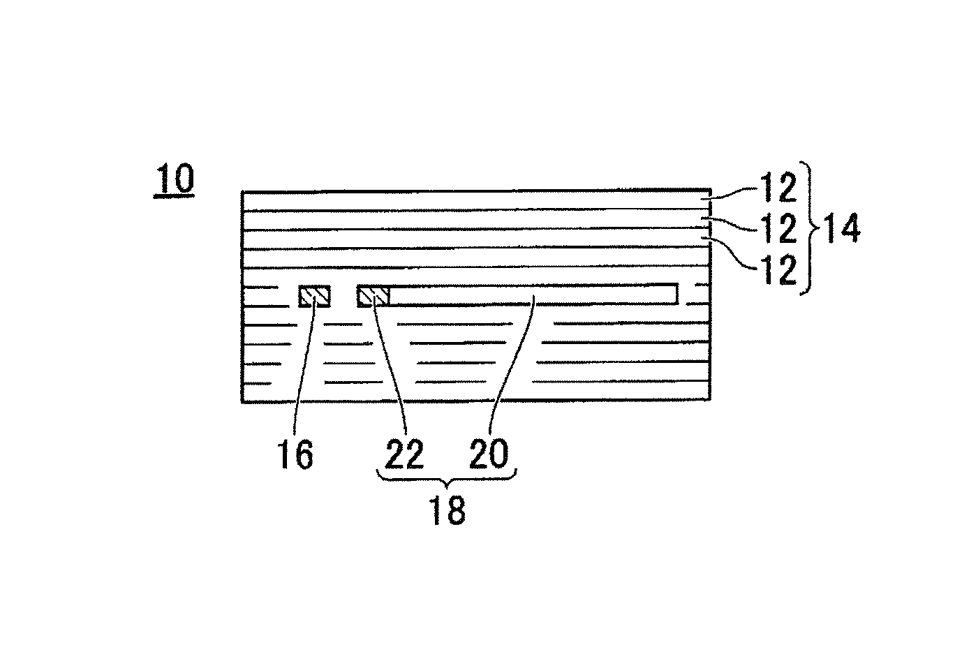
[0026]The electronic component 10 of the first embodiment functions as the electronic component 10 when there is only the multilayer ceramic substrate 14 and functions as an electronic component module when an electronic component element (not illustrated) is mounted on the multilayer ceramic substrate 14.
[0027]The material of the ceramic layers 12 is preferably one including barium oxide, silicon oxide or alumina as a main component. In addition, instead of that, a material obtained by for example adding a glass component, which acts as a sintering additive, to a material acting as a ceramic filler such as alumina or barium titanate may be used as the material of the ceramic layers 12. However, in the case where a reducing atmosphere is necessary in the firing conditions due to the material characteristics of for example an electrode material to be described later, a composition that is not reduced when fired in the reducing atmosphere needs to be selected.
[0028]In the electronic c...
second embodiment
[0042]Similarly to the electronic component 10, the electronic component 10′ of the second embodiment functions as the electronic component 10′ when there is only the multilayer ceramic substrate 14 and functions as an electronic component module when an electronic component element (not illustrated) is mounted on the multilayer ceramic substrate 14.
[0043]In the electronic component 10′ of the second embodiment, the wiring electrode 16 and the planar electrode 18 are both formed on the same ceramic layer 12. The wiring electrode 16 is linearly formed on the ceramic layer 12. The planar electrode 18 is planarly formed so as to be adjacent to and spaced apart from the wiring electrode 16 at a certain interval. An edge portion 22a is formed in a region of the planar electrode 18 that is adjacent to and spaced apart from the wiring electrode 16 at the certain interval. In addition, an edge portion 22b is formed in a region that is on the opposite side to the region of the planar electro...
PUM
| Property | Measurement | Unit |
|---|---|---|
| width | aaaaa | aaaaa |
| width | aaaaa | aaaaa |
| width | aaaaa | aaaaa |
Abstract
Description
Claims
Application Information