
OTP memory cell, OTP memory, and method of manufacturing OTP memory cell

a technology of memory cells and memory cells, which is applied in the field of manufacturing otp memory cells, can solve the problems of increasing chip area and breaking down of otp cells, and achieve the effects of low breakdown resistance, small transistors, and low breakdown resistance voltag

Inactive Publication Date: 2008-11-20
RENESAS ELECTRONICS CORP
View PDF5 Cites 9 Cited by
  • Summary
  • Abstract
  • Description
  • Claims
  • Application Information

AI Technical Summary

Benefits of technology

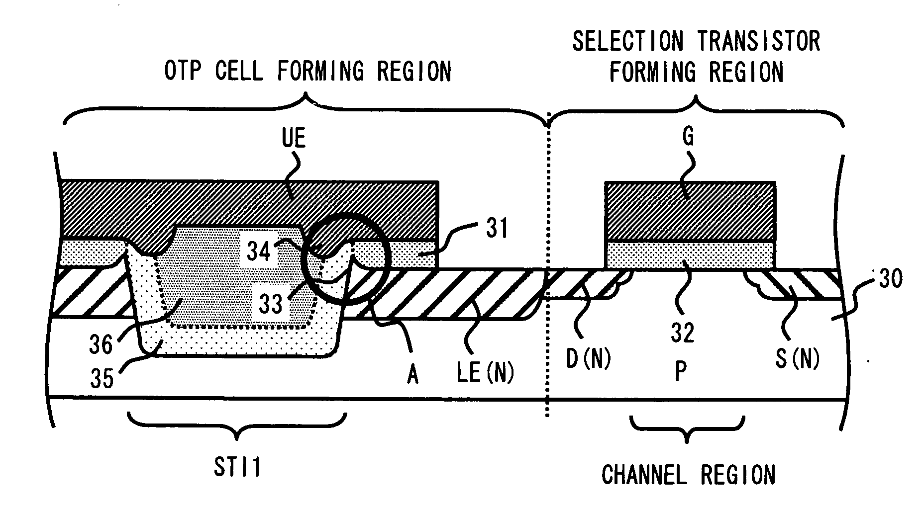
[0010]With the OTP memory cell according to the present invention, the shape of at least a part of the end of the lower electrode forming region in contact with the first insulating film is sharper than the shape of the end of the channel region in contact with the second insulating film. Accordingly, during destructive write of the state memory cell, an electric field having a strength greater than that of an electric field generated in the channel region of the selection transistor is generated at a sharp portion formed at the end of the lower electrode. As a result, a withstand voltage of the state memory cell becomes lower than a breakdown withstand voltage of the selection transistor at the sharp portion.
[0011]Further, an OTP memory according to the present invention includes the above-described OTP memory cells. In other words, it is possible to set the breakdown withstand voltage of the state memory unit to be lower than that of a conventional state memory cell. Accordingly, there is no need to generate a voltage higher than that of a peripheral circuit of the memory cell, and there arises no problem if the withstand voltage of an element constituting the peripheral circuit is lowered.
[0012]With the OTP memory cell, the OTP memory, and the method of manufacturing an OTP memory cell according to the present invention, it is possible to set the breakdown withstand voltage of the OTP cell to be lower than that of the conventional OTP cell. As a result, the breakdown withstand voltage of each of the selection transistor and a transistor constituting a peripheral circuit can be set to be lower than that of the conventional case. Accordingly, with the OTP memory cell, the OTP memory, and the method of manufacturing an OTP memory cell according to the present invention, the selection transistor and the peripheral circuit can be formed using a transistor having a small transistor size and a low breakdown withstand voltage, whereby the reduction in circuit area can be achieved.

Problems solved by technology

However, in Related Art 1, the voltage high enough to cause the breakdown in the OTP cell is applied.
Accordingly, when a circuit incorporating such a high withstand voltage element is additionally provided, there arises a problem of an increase in chip area.

Method used


Image

  • OTP memory cell, OTP memory, and method of manufacturing OTP memory cell
  • OTP memory cell, OTP memory, and method of manufacturing OTP memory cell
  • OTP memory cell, OTP memory, and method of manufacturing OTP memory cell

Examples


first embodiment

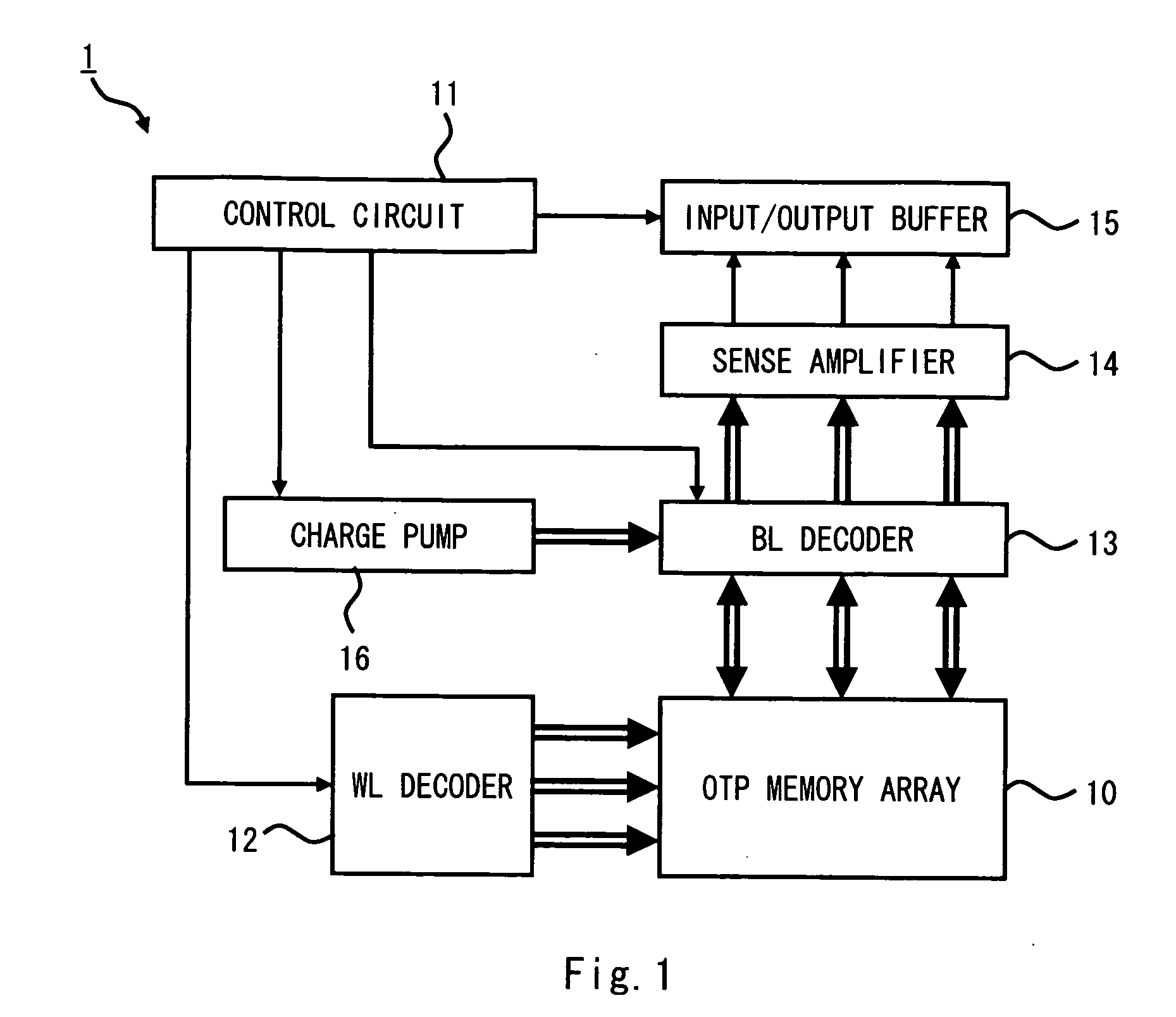
[0062]Hereinafter, embodiments of the present invention will be described with reference to the drawings. In the following description, as an example of a semiconductor device according to the present invention, a description is given of an OTP memory incorporating an OTP memory cell as a state memory cell. FIG. 1 is a block diagram showing a semiconductor device 1 according to a first embodiment of the present invention. As shown in FIG. 1, the semiconductor device 1 includes an OTP memory array 10, a control circuit 11, a WL decoder 12, a BL decoder 13, a sense amplifier 14, an input / output buffer 15, and a charge pump 16.

[0063]The OTP memory array 10 includes a plurality of OTP memory cells each having a state memory cell. In the OTP memory array 10, the plurality of OTP memory cells are arranged in a lattice manner. The OTP memory array 10 will be described in detail later. The control circuit 11 controls each block incorporated in the semiconductor device 1 in response to a con...

second embodiment

[0111]FIGS. 30A to 30C are cross-sectional diagrams each showing an OTP memory cell according to a second embodiment of the present invention, which correspond to the cross-sectional diagrams of FIGS. 5A to 5C each showing the OTP memory cell according to the first embodiment. As shown in FIGS. 30A to 30C, the OTP cell according to the second embodiment has a hollow portion 38 in the side wall in contact with the first trench-type insulating region STI1 of the lower electrode LE. In this case, each sharp portion having the hollow portion 38 is referred to as a sharp portion 37.

[0112]The sharp portion 37 having the hollow portion 38 is thinner than the sharp portion 33 of the first embodiment. As a result, the strength of an electric field concentrated on the sharp portion 37 is greater than that on the sharp portion 33. Accordingly, the OTP cell of the second embodiment has a breakdown withstand voltage lower than that of the OTP cell of the first embodiment.

[0113]The hollow portion...

third embodiment

[0115]A third embodiment of the present invention is a modified example of the OTP cell of the first embodiment. Accordingly, the components identical with those of the first embodiment are omitted. FIG. 32 shows a circuit diagram of the OTP memory cell according to the third embodiment.

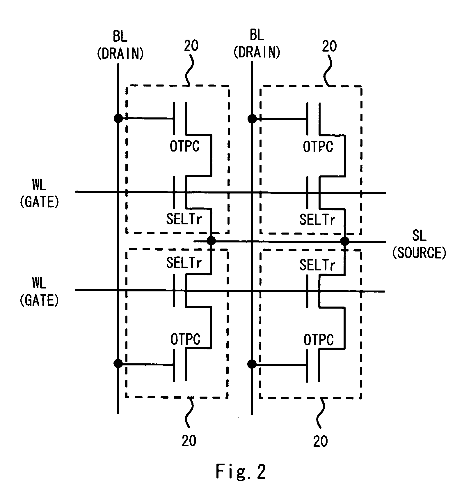
[0116]As shown in FIG. 32, the OTP memory cell of the third embodiment includes a plurality of OTP memories 60. The OTP memories 60 each include a selection transistor (represented as SELTr of FIG. 32) and an OTP cell (represented as OTPC of FIG. 32). A gate of the selection transistor is connected to the word line WL, and a drain of the selection transistor is connected to the bit line BL. A source of the selection transistor is connected to an upper electrode of the OTP cell. A lower electrode of the OTP cell is connected to the source line SL. FIG. 33 shows a planar layout of the OTP memories 60.

[0117]As shown in FIG. 33, in the OTP memory cell of the third embodiment, the lower electrode LE is fo...


PUM


Abstract

An OTP memory cell according to the present invention includes: a semiconductor substrate including a lower electrode forming region having a lower electrode formed therein, a diffusion layer forming region having a source and a drain formed therein, a first trench-type insulating region, and a second trench-type insulating region; an upper electrode being in contact with the first trench-type insulating region and formed on the lower electrode with the first insulating film interposed therebetween; and a gate electrode being in contact with the second trench-type insulating region and formed on a channel region with the second insulating film interposed therebetween, in which a shape of at least a part of an end of the lower electrode forming region in contact with the first insulating film is sharper than a shape of an end of the channel region in contact with the second insulating film.

Description

BACKGROUND OF THE INVENTION[0001]1. Field of the Invention[0002]The present invention relates to a one time programmable (OTP) memory cell, an OTP memory, and a method of manufacturing an OTP memory cell. In particular, the present invention relates to an OTP memory cell having a nonvolatile state memory cell that is writable only once, an OTP memory, and a method of manufacturing an OTP memory cell.[0003]2. Description of Related Art[0004]As an example of a nonvolatile state memory cell formed in a semiconductor device, there is known a one time programmable cell (hereinafter, referred to as “OTP cell”) that is writable only once. Japanese Patent Translation Publication No. 2005-504434 (hereinafter, referred to as “Related Art 1”) discloses an example of a memory cell having the OTP cell. FIG. 47 shows a cross-sectional diagram of a memory cell 100 having the OTP cell as disclosed in Related Art 1.[0005]The memory cell 100 includes an OTP cell and a selection transistor. FIG. 47 sh...

Claims


Application Information

Patent Timeline
Patent Type & Authority Applications(United States)
IPC IPC(8): H01L27/112
CPCG11C17/16H01L27/10H01L27/105H01L27/11206H01L27/11286H01L27/1052H10B20/60H10B20/25
Inventor WADA, MASAHIRO
Owner RENESAS ELECTRONICS CORP
Learn More