Plasma based ion implantation system

a technology of ion implantation and plasma, which is applied in the direction of chemical vapor deposition coating, coating, electric discharge tube, etc., can solve the problems of reducing the productivity of semiconductor devices, ion and radicals are excessively generated, and different plasma generation schemes, so as to reduce unnecessary ionization and dissociation, improve process efficiency, and ensure the effect of uniform plasma

Inactive Publication Date: 2008-11-27
SAMSUNG ELECTRONICS CO LTD
View PDF15 Cites 55 Cited by
  • Summary
  • Abstract
  • Description
  • Claims
  • Application Information

AI Technical Summary

Benefits of technology

[0011]Accordingly, it is an aspect of the present invention to provide a plasma based ion implantation system capable of performing an effective discharge in a wide process region while solving

Problems solved by technology

However, when using a conventional ion implantation technology based on ion beam line (BL), the productivity of the semiconductor devices is significantly reduced to satisfy the above process condition.
However, they represent difference in plasma generation schemes.
However, if the inductively plasma generator is used for the PBII process, the following problems occur.
However, the inductively coupled plasma has an electron temperature higher than that of capacitively coupled plasma, so that ions and rad

Method used


Image

  • Plasma based ion implantation system
  • Plasma based ion implantation system
  • Plasma based ion implantation system

Examples


Embodiment Construction

[0026]Reference will now be made in detail to the embodiments of the present invention, examples of which are illustrated in the accompanying drawings, wherein like reference numerals refer to the like elements throughout. The embodiments are described below to explain the present invention by referring to the figures.

[0027]Hereinafter, a preferred embodiment of the present invention will be described in detail with reference to the accompanying drawings.

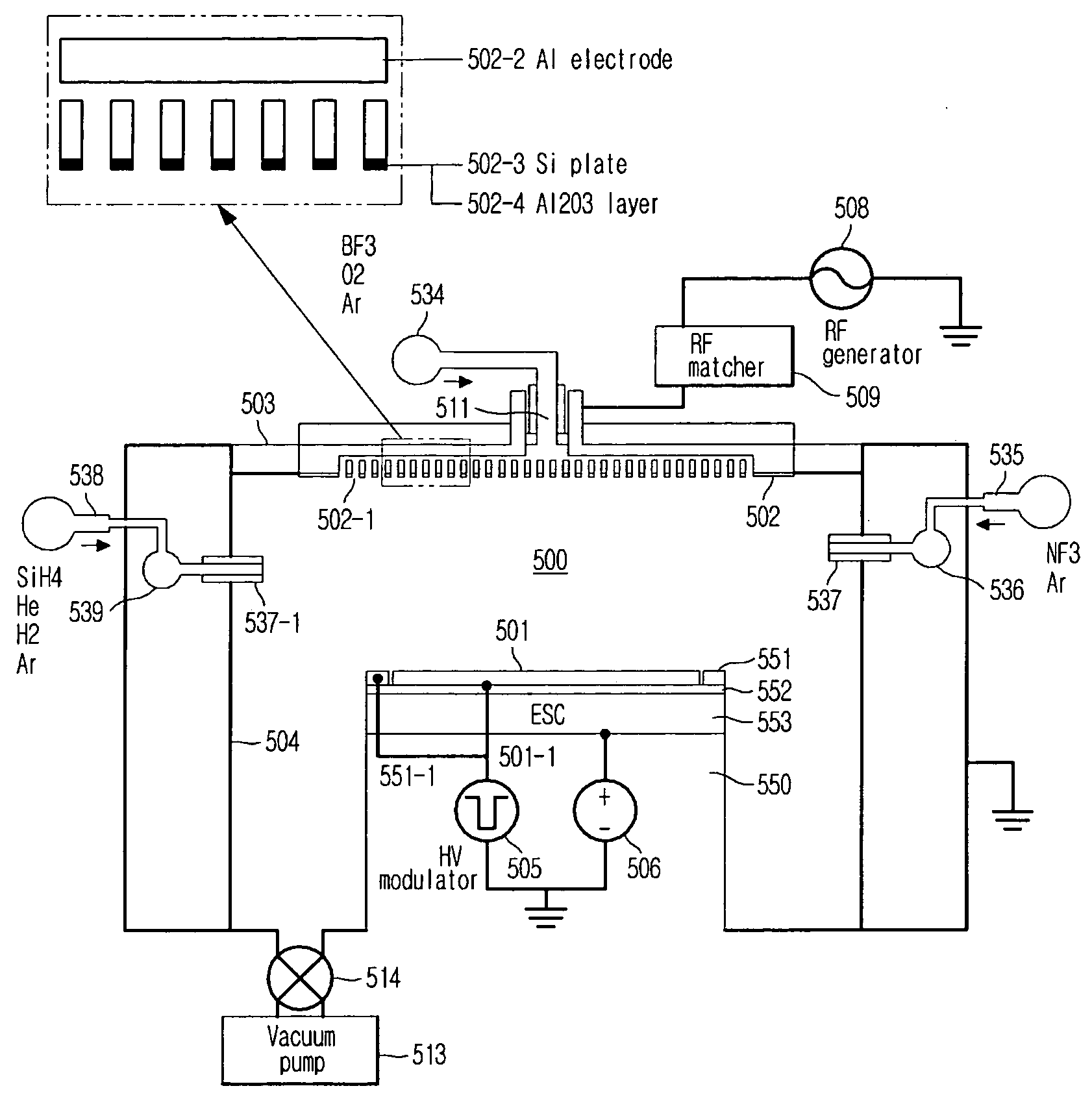
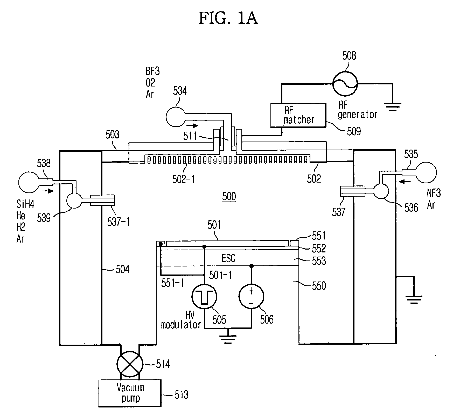
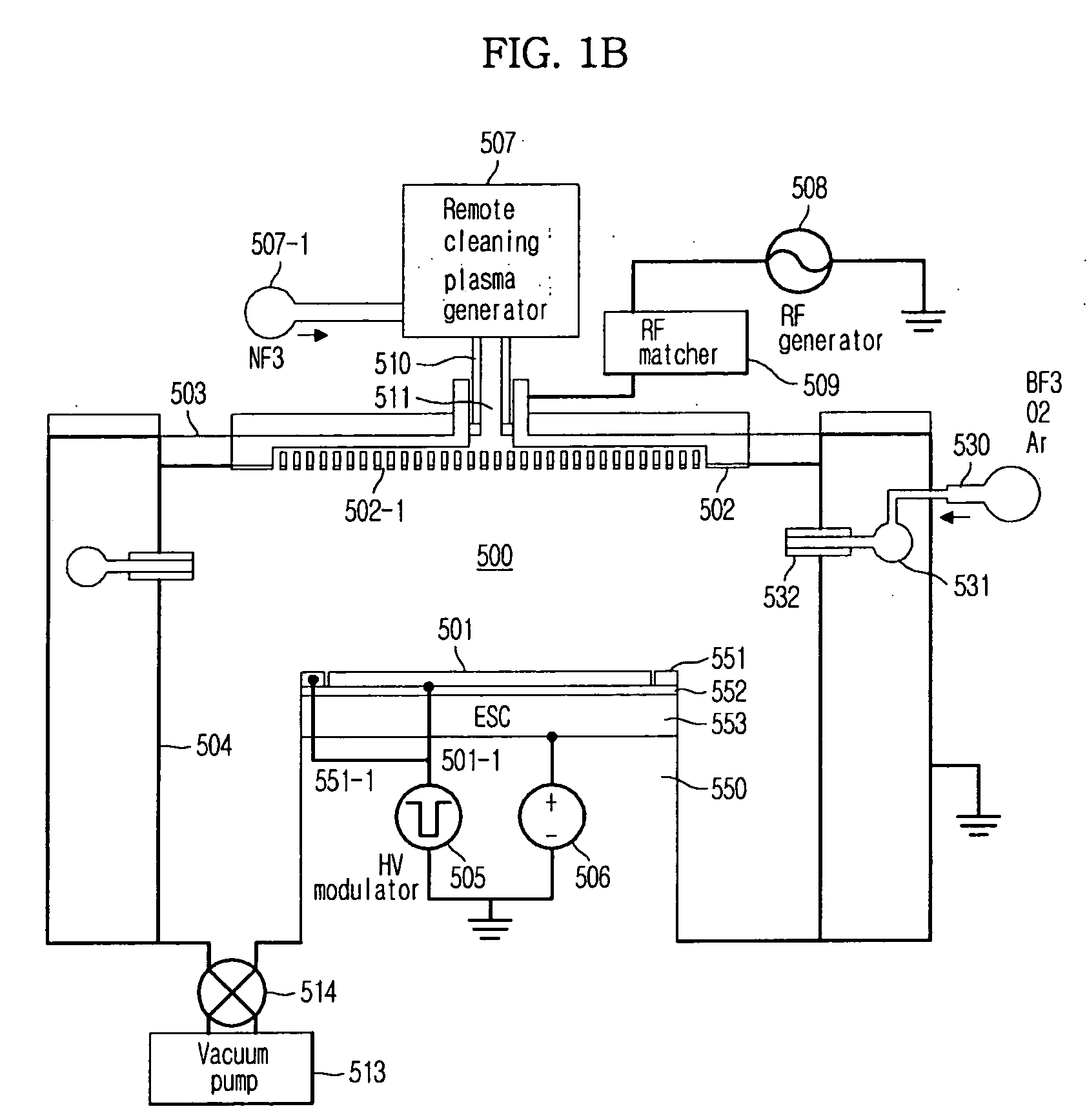
[0028]A plasma based ion implantation system according to an embodiment of the present invention is illustrated in FIGS. 1A to 4. As shown in FIG. 1A, a workpiece 501 is positioned on a lower electrode 553 in a vacuum chamber 500. The vacuum chamber 500 includes a sidewall 504 and a ceiling 503 having an RF capacitively coupled upper electrode 502. The sidewall 504 of the vacuum chamber 500 has an area larger than that of workpiece 501. The upper electrode 502 is disposed at a front portion of the workpiece 501 while being spaced ap...


PUM

PropertyMeasurementUnit
Timeaaaaaaaaaa
Timeaaaaaaaaaa
Timeaaaaaaaaaa

Abstract

A plasma based ion implantation system capable of generating a capacitively coupled plasma having beneficial characteristics for an ion implantation, including the generation of necessary ions and radicals only for an ion implantation process instead of generating an inductively coupled plasma, which generates unnecessary ions and excessively dissociates radicals. The plasma based ion implantation system easily controls plasma ions implanted by cleaning a vacuum chamber, minimizes problems of unnecessary deposition and occurrence of contaminants and increases the number of components used only for the plasma ion implantion by reducing the deposition of polymer layer on a workpiece. The plasma based ion implantation system easily control uniformity of the plasma by using a flat type electrode, thereby easily ensuring uniformity of plasma ions implanted into the workpiece.

Description

CROSS-REFERENCE TO RELATED APPLICATIONS[0001]This application claims the benefit of Korean Patent Application No. 10-2007-0050132 filed on May 23, 2007, in the Korean Intellectual Property Office, the disclosure of which is incorporated herein by reference.BACKGROUND[0002]1. Field[0003]The present invention relates to a plasma based ion implantation system. More particularly, the present invention relates to a plasma based ion implantation system capable of controlling an implantation of ions in an easy way as compared with an ion beam based ion implantation and reducing a problem of unnecessary deposition, and contamination on a surface of a wafer.[0004]2. Description of the Related Art[0005]A plasma based ion implantation (PBII) technology is a core technology, which is essentially necessary to develop a semiconductor device having a line width of 80 nm or below. The PBII technology is an ion doping technology for a Si device for realizing a CMOS (complimentary metal oxide semicon...

Claims


Application Information

Patent Timeline
IPC IPC(8): C23C16/44
CPCH01J37/32357H01J37/32412H01J37/3244H01J37/32449H01J37/3255H01J37/32862H01L21/2236H01L21/265
Inventor LEE, YOUNG DONGTOLMACHEV, YURIVOLYNETS, VLADIMIRPASHKOVSKIY, VASILYUSHAKOV, ANDREYKEUM, GYEONG SUHAN, JAE HYUNKIM, DONG CHEOLCHO, HYUNG CHUL
Owner SAMSUNG ELECTRONICS CO LTD
Why Eureka
Try Eureka