
Multilayer inductor component

a technology of inductor components and inductances, applied in the direction of transformers/inductances, magnetic cores, inductances, etc., can solve the problems of high frequency noise and achieve the effect of eliminating noise, raising impedances, and increasing frequencies

Active Publication Date: 2008-12-04
TDK CORPARATION
View PDF2 Cites 3 Cited by
  • Summary
  • Abstract
  • Description
  • Claims
  • Application Information

AI Technical Summary

Benefits of technology

[0006]Recently, as electronic devices such as personal computers, cellular phones, and devices related to DSC, LCD, and DVD have been operating at higher frequencies, their noise has also been reaching higher frequencies. Therefore, demands have been increasing for EMC components (noise eliminating components for signal lines) which can acutely raise their impedances in high-frequency bands (e.g., 1 GHz or higher) so as to eliminate noise and can lower the impedances unnecessary for passing signals in low-frequency bands (e.g., 100 MHz or lower). Namely, it has been demanded to extend the frequency characteristic of their impedances to the higher frequency side than that conventionally attainable.
[0007]It is an object of the present invention to provide a multilayer inductor component which can eliminate noise in a high-frequency band.
[0010]In the multilayer inductor component in accordance with the present invention, the magnetic layers have the composition mentioned above, while the impedance peak value in the high-frequency band of 1 GHz or higher is 500Ω or greater. Namely, the multilayer inductor component in accordance with the present invention can shift the series resonance frequency to the higher frequency side (1 GHz or higher) than that conventionally attainable. As a result, when mounted in electronic devices, the multilayer inductor component in accordance with the present invention can eliminate noise occurring in the high-frequency band.
[0012]The present invention can provide a multilayer inductor component which can eliminate noise in the high-frequency band.

Problems solved by technology

Recently, as electronic devices such as personal computers, cellular phones, and devices related to DSC, LCD, and DVD have been operating at higher frequencies, their noise has also been reaching higher frequencies.

Method used


Image

  • Multilayer inductor component
  • Multilayer inductor component
  • Multilayer inductor component

Examples


example 1

Making of Multilayer Chip Bead

[0051]In the following manner, the multilayer chip bead of Example 1 was made according to the above-mentioned manufacturing method.

[0052]First, in the making of the multilayer chip bead, a mixed powder of a ferrite powder and an additive was prepared. In the making of the ferrite powder, 30.0 mol % of Fe2O3, 58.0 mol % of NiO, 9.0 mol % of CuO, and 3.0% of Zn were weighed, so as to yield a raw material powder. The raw material powder with 0.1 mass % (1,000 ppm) of CoO as an additive added thereto was wet-mixed with deionized water in a ball mill and then dried with a spray dryer, whereby a mixed powder was obtained. Subsequently, the mixed powder was temporarily fired at 700 to 800° C. for 10 hr, so as to yield a temporarily fired powder. Thereafter, the temporarily fired powder was wet-mixed with deionized water in a ball mill and then pulverized until particles having an average particle size of 0.7 μm with a specific surface area on the order of 5 t...


PUM

PropertyMeasurementUnit
Percent by massaaaaaaaaaa
Electrical resistanceaaaaaaaaaa
Frequencyaaaaaaaaaa

Abstract

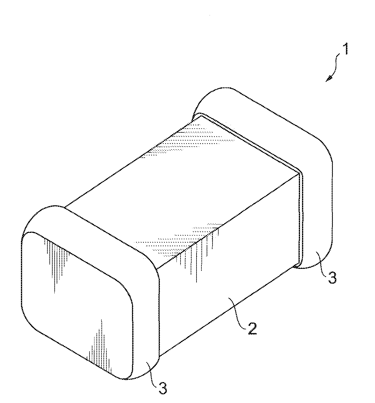
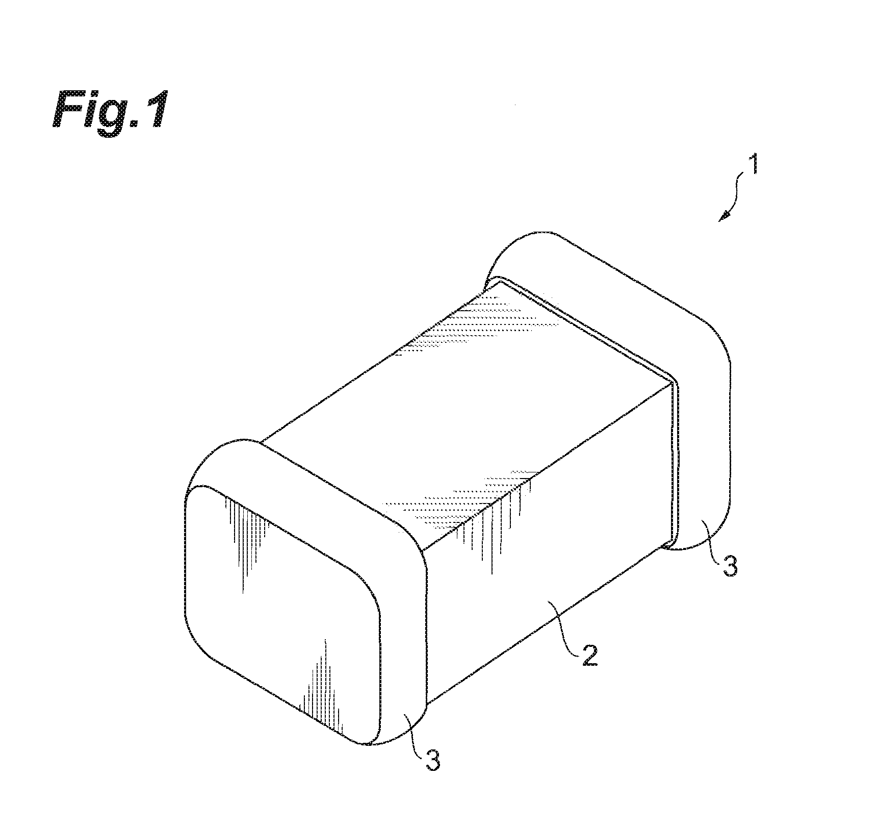
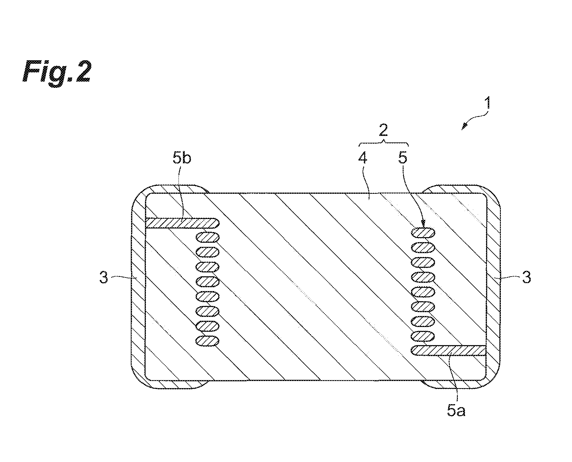
A multilayer inductor component has a multilayer part having a plurality of magnetic layers laminated therein and a conductor part arranged within the multilayer part. The magnetic layers are formed from a ferrite material and an additive. The ferrite material contains Fe2O3, NiO, CuO, and ZnO. Fe2O3 is 30 to 45 mol %. NiO is 45 to 58 mol %. CuO is 6 to 10 mol %. ZnO is 0 to 3 mol %. The additive contains CoO. The content of CoO is 0.1 to 2.5 mass % with respect to the ferrite material as a whole. The multilayer inductor component has an impedance peak of 500Ω or greater at an operating frequency of 1 GHz or higher.

Description

BACKGROUND OF THE INVENTION[0001]1. Field of the Invention[0002]The present invention relates to a multilayer inductor component.[0003]2. Related Background Art[0004]In general, a multilayer inductor component such as chip inductor, chip bead, chip transformer, or LC composite chip comprises a multilayer part in which magnetic layers are laminated, and a conductor part having a coil-like structure arranged within the multilayer part.[0005]As an example of the multilayer inductor component, Japanese Patent No. 3421656 (Japanese Patent Application Laid-Open No. 2002-246217) discloses a chip inductor constituted by a ferrite material containing 25 to 52 mol % of Fe2O3, 0 to 40 mol % of ZnO, 0 to 20 mol % of CuO, and 1 to 65 mol % of NiO.SUMMARY OF THE INVENTION[0006]Recently, as electronic devices such as personal computers, cellular phones, and devices related to DSC, LCD, and DVD have been operating at higher frequencies, their noise has also been reaching higher frequencies. Therefo...

Claims


Application Information

Patent Timeline
IPC IPC(8): H01F1/047
CPCH01F1/0027H01F1/344H01F17/0013H01F17/0033H01F41/046
Inventor SUTOH, NAOKISUZUKI, TAKASHIODA, KUNIOTAKAHASHI, YUKIOKAWASAKI, KUNIHIKOMOMOI, HIROSHI
Owner TDK CORPARATION
Learn More