Method for manufacturing substrate for semiconductor light emitting element and semiconductor light emitting element using the same

a technology of light emitting elements and manufacturing substrates, applied in semiconductor/solid-state device manufacturing, semiconductor devices, electrical devices, etc., can solve the problems of low external quantum efficiency, cracks and/or other trouble, partial breakage of p-n junctions, etc., to achieve excellent optical properties, no need to increase the number of processes, and excellent mass productivity

Active Publication Date: 2008-12-11
NICHIA CORP
View PDF8 Cites 135 Cited by
  • Summary
  • Abstract
  • Description
  • Claims
  • Application Information

AI Technical Summary

Benefits of technology

[0022]The semiconductor light emitting element of the present invention is capable of preferable light extracting by the optical structure of the substrate thereof. Further, in a manufacture of the substrate of the element having a complicated shape with excellent optical properties, the number of processes is not needed to be increased while ex

Problems solved by technology

A part of light is absorbed during the propagation, resulting in lower external quantum efficiency.
A method of roughing the top surface and side surfaces of the light emitting diode chip has been proposed, but it may cause damage on the semiconductor layer and results in cracks and/or other trouble.
This leads to partial breakage of p-n juncti

Method used


Image

  • Method for manufacturing substrate for semiconductor light emitting element and semiconductor light emitting element using the same
  • Method for manufacturing substrate for semiconductor light emitting element and semiconductor light emitting element using the same
  • Method for manufacturing substrate for semiconductor light emitting element and semiconductor light emitting element using the same

Examples


embodiment 1

Semiconductor Light Emitting Element and Substrate Thereof

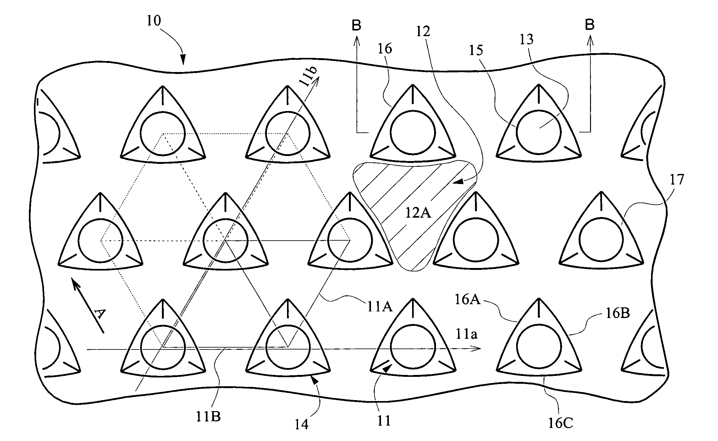
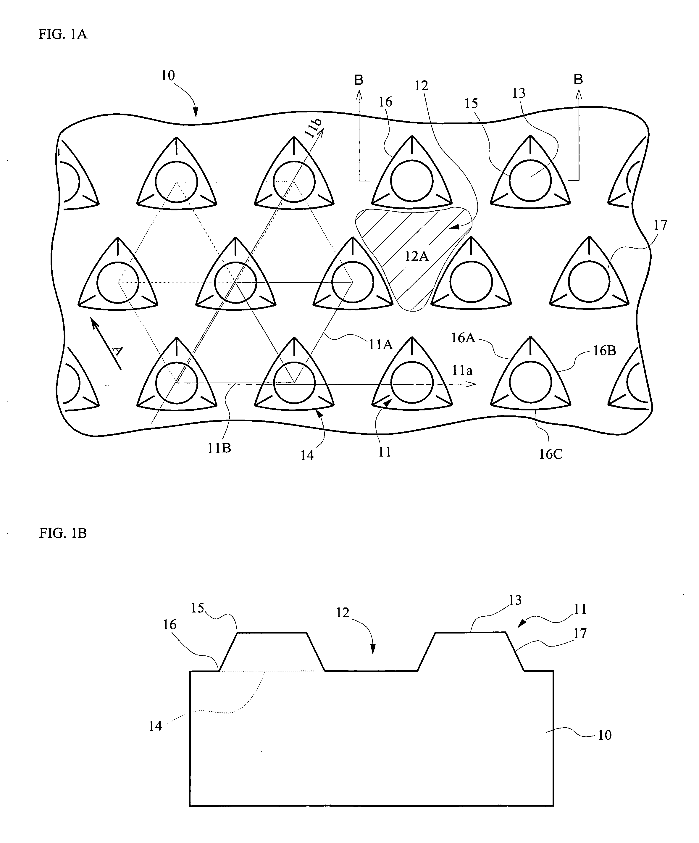
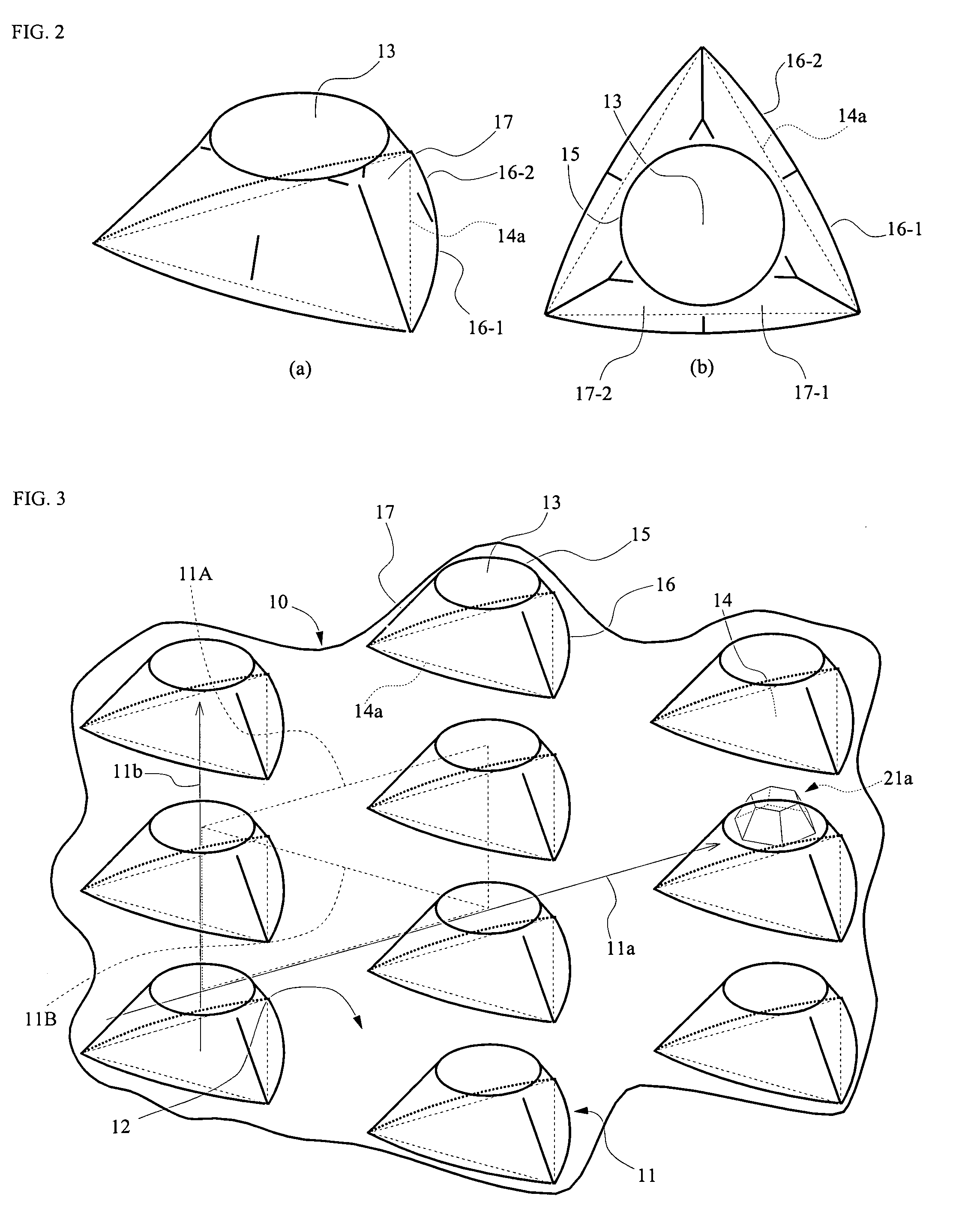
[0042]A semiconductor light emitting element of the present invention has, as shown in FIG. 9 and the like, basically, a light emitting element structure made of a semiconductor layered structure 20 is provided on a substrate 10. A structure having optical function such as reflection and / or refraction of light corresponding to light from the light emitting element is provided mainly on a semiconductor side of a semiconductor growth substrate 10 (a first main surface). Specifically, as shown in FIG. 9, a recess / protrusion structure 11 is provided on a first main surface of the substrate. The recess / protrusion forms an interface having an optical function with a semiconductor having different refractive index than that of the substrate so as to reflect and / or refract light propagating in lateral direction (shown by an outline arrow in the figure) at the recesses or protrusions, especially at an inclined side surface, as indicat...

embodiment 2

Method of Manufacturing Substrate and Element Using the Substrate

[0061]A method of manufacturing the above-described substrate and element will be illustrated in Embodiment 2 below and a substrate for light emitting element and an element will be illustrated thereafter.

[0062]In a method of manufacturing above-described protrusions shown in FIGS. 1 to 4, as shown in FIG. 7, a mask 19 is formed on the substrate and the protrusions with a top surface, bottom surface and side surface, each having a desired shape described above, are formed by etching the substrate.

[0063]Examples of etching include wet etching and dry etching that will be described hereinafter. As a dry etching, vapor phase etching, plasma etching, or reactive ion etching may be employed. Examples of the etching gas include, a chlorine-based gas and a fluorine-based gas such as Cl2, SiCl4, BCl3, HBR, SF6, CHF3, C4F8, CF4 and the like, and an inactive gas such as Ar.

[0064]In the cases where dry etching is employed, as sho...

example 1

[0098]A sapphire substrate having a principal plane in C-plane (0 0 0 1) and an orientation flat surface in A-plane (1 −1 2 0) is used. First, a SiO2 film 19 that makes an etching mask is formed on the sapphire substrate 10, as shown in FIG. 7A(a). Then, using a photomask, masks 19 each having circular shape of about 2 μm in diameter are arranged periodically.

[0099]Then, as shown in FIG. 7A(b), the substrate is immersed in an etching bath containing a mixed acid of phosphoric acid and sulfuric acid as etchant at about 290° C. for about 5 minutes to obtain a depth (height of protrusions) of about 1.1 μm.

[0100]The structure of a protrusion thus obtained on the substrate may have a structure, as shown in FIG. 1A, in which a side of a triangle of the bottom surface 14 is about 3 μm and each of the two sides 16-1, 16-2 forming a constituent side 16 thereof shown in FIG. 2 is about 1.5 μm. Such protrusions are arranged periodically with intervals of the protrusions 11 of about 3 μm, that ...


PUM


Abstract

A light emitting element having a recess-protrusion structure on a substrate is provided. A semiconductor light emitting element 100 has a light emitting structure of a semiconductor 20 on a first main surface of a substrate 10. The first main surface of the substrate 10 has substrate protrusion portion 11, the bottom surface 14 of each protrusion is wider than the top surface 13 thereof in a cross-section, or the top surface 13 is included in the bottom surface 14 in a top view of the substrate. The bottom surface 14 has an approximately polygonal shape, and the top surface 13 has an approximately circular or polygonal shape with more sides than that of the bottom surface 14.

Description

BACKGROUND OF THE INVENTION[0001]1. Technical Field[0002]The present invention relates to a semiconductor device having a recess or protrusion (hereinafter may be referred to as recess / protrusion) provided on a substrate and, more particularly, to a semiconductor light emitting element that improves its external quantum efficiency by having the recess or protrusion provided on the substrate, and a substrate used therein and a method of manufacturing them.[0003]2. Background Art[0004]A semiconductor element, i.e., a light emitting diode (LED) basically comprises an n-type semiconductor layer, an active layer and a p-type semiconductor layer stacked on a substrate in this order, and electrodes are formed thereon. Light from the active layer is discharged outside of the element from such as outwardly exposed surfaces (top surface, side surface) of the semiconductor structure and exposed surfaces (back surface, side surface) of the substrate.In detail, when light generated in the semico...

Claims


Application Information

Patent Timeline
IPC IPC(8): H01L33/00H01L33/22H01L33/32H01L33/60H01L33/62
CPCH01L33/10H01L33/24H01L2224/48247H01L2224/48465H01L2924/01012H01L2924/0102H01L2924/01046H01L2924/01057H01L2924/01063H01L2924/01077H01L2924/01078H01L2924/01079H01L2924/01019H01L2924/01322H01L33/20H01L33/32H01L2924/00H01L2224/48095
Inventor MINATO, SHUNSUKENARITA, JUNYAWAKAI, YOHEINARUKAWA, YUKIOYAMADA, MOTOKAZU
Owner NICHIA CORP
Why Eureka
Try Eureka