Method of driving ccd solid-state image pickup device, and image pickup apparatus

Inactive Publication Date: 2008-12-18
FUJIFILM CORP
View PDF1 Cites 6 Cited by
  • Summary
  • Abstract
  • Description
  • Claims
  • Application Information

AI Technical Summary

Benefits of technology

[0020]It is a first object of the invention to provide a method of driving a CCD solid-state image pickup device, and image pickup

Problems solved by technology

However, the floating diffusion amplifier (FDA) 14 and subsequent stage circuits which are disposed in the output stage of the CCD solid-state image pickup device are susceptible to noises.
Even when signal amplification is performed in the output stage, it is impossible to obtain an amplification output of a high S/N ratio.
When semiconductors and electrodes are configured by a material or structure which is highly resistant, however, there arises a problem in that the production cost is increased.
However, there is a problem in that, in a configuration where a high voltage is simply applied to the electrode V3 to form a deep potential well, all electrodes in the packet 19 cannot be rapidly moved int

Method used


Image

  • Method of driving ccd solid-state image pickup device, and image pickup apparatus
  • Method of driving ccd solid-state image pickup device, and image pickup apparatus
  • Method of driving ccd solid-state image pickup device, and image pickup apparatus

Examples


first embodiment

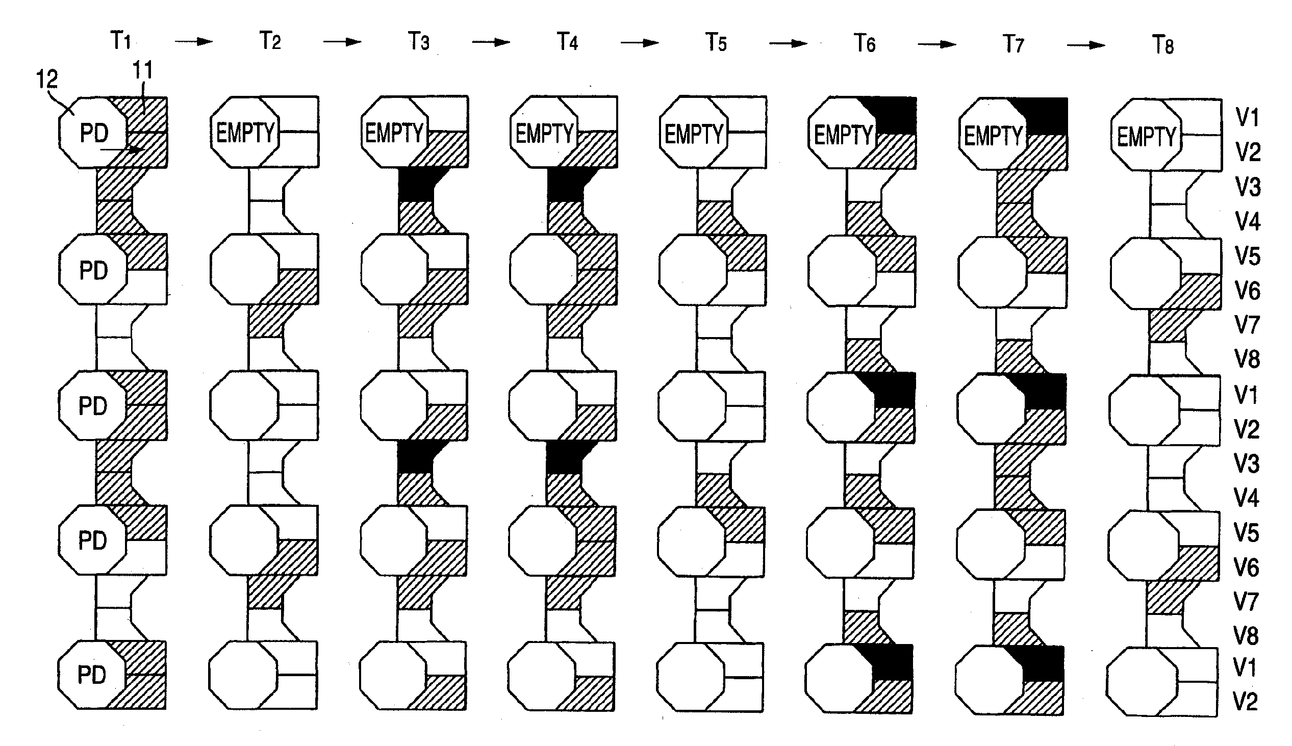
[0085]FIG. 1 is a diagram illustrating a method of driving a CCD solid-state image pickup device of a first embodiment of the invention. The illustrated solid-state image pickup device is an image pickup device which has a honeycomb pixel arrangement shown in FIG. 21A. The figure shows a change of states (T1 to T8) of one pixel (PD) column and vertical charge transfer path of the device.

[0086]Among the illustrated transfer electrodes adjacent to the pixels PD, electrodes V2, V6 are transfer electrodes which function also as a readout electrode. When a high voltage is applied to the readout electrodes, accumulated charges in pixels PD are read out to the vertical charge transfer path. As shown in FIG. 21A, in the honeycomb pixel arrangement, the pixel column next to the pixel column shown in FIG. 1 is staggered by ½ pitch. In the next pixel column, therefore, the readout electrodes are electrodes V4, V8.

[0087]When a high voltage is applied to the electrodes V4, V8, accumulated charge...

second embodiment

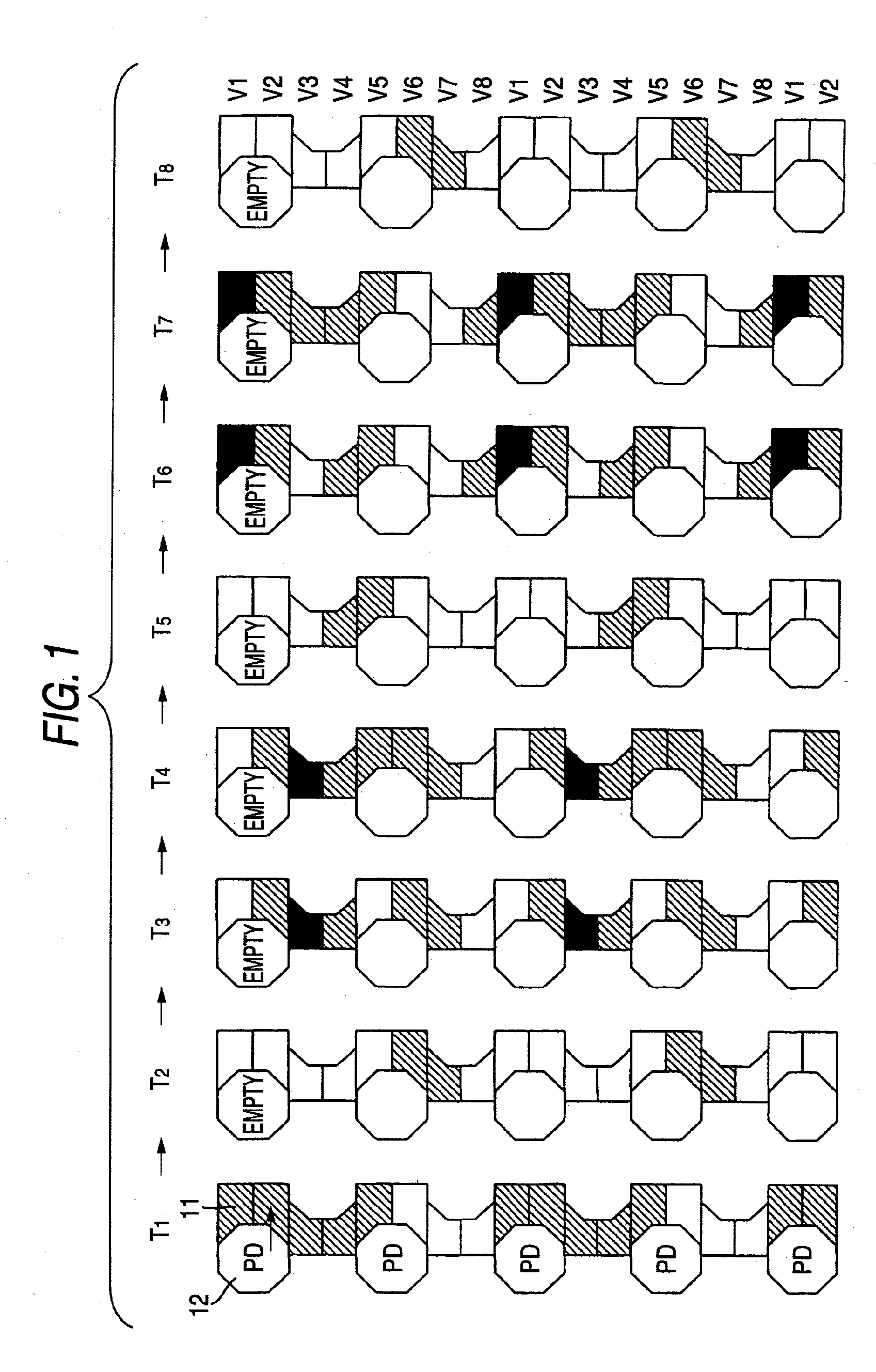
[0101]FIGS. 4 to 6 are diagrams illustrating a method of driving a CCD solid-state image pickup device of a second embodiment of the invention. The figures correspond to FIGS. 1 to 3 in the first embodiment, respectively. In the embodiment, a driving method similar to that of the first embodiment is applied to the CCD solid-state image pickup device shown in FIG. 21B.

[0102]In the illustrated example, among the transfer electrodes adjacent to the pixels PD, electrodes V1, V3, V5, V7 are transfer electrodes which function also as a readout electrode. When a high voltage is applied to the readout electrodes, accumulated charges in pixels PD are read out to the vertical charge transfer path. In a state where a signal charge is already read out from a corresponding pixel and the pixel is empty, even when a high voltage is applied to a readout electrode, however, no signal charge is read out.

[0103]In FIG. 4, the meanings of “hollow”, “hatched”, and “solid” in the vertical transfer electro...

third embodiment

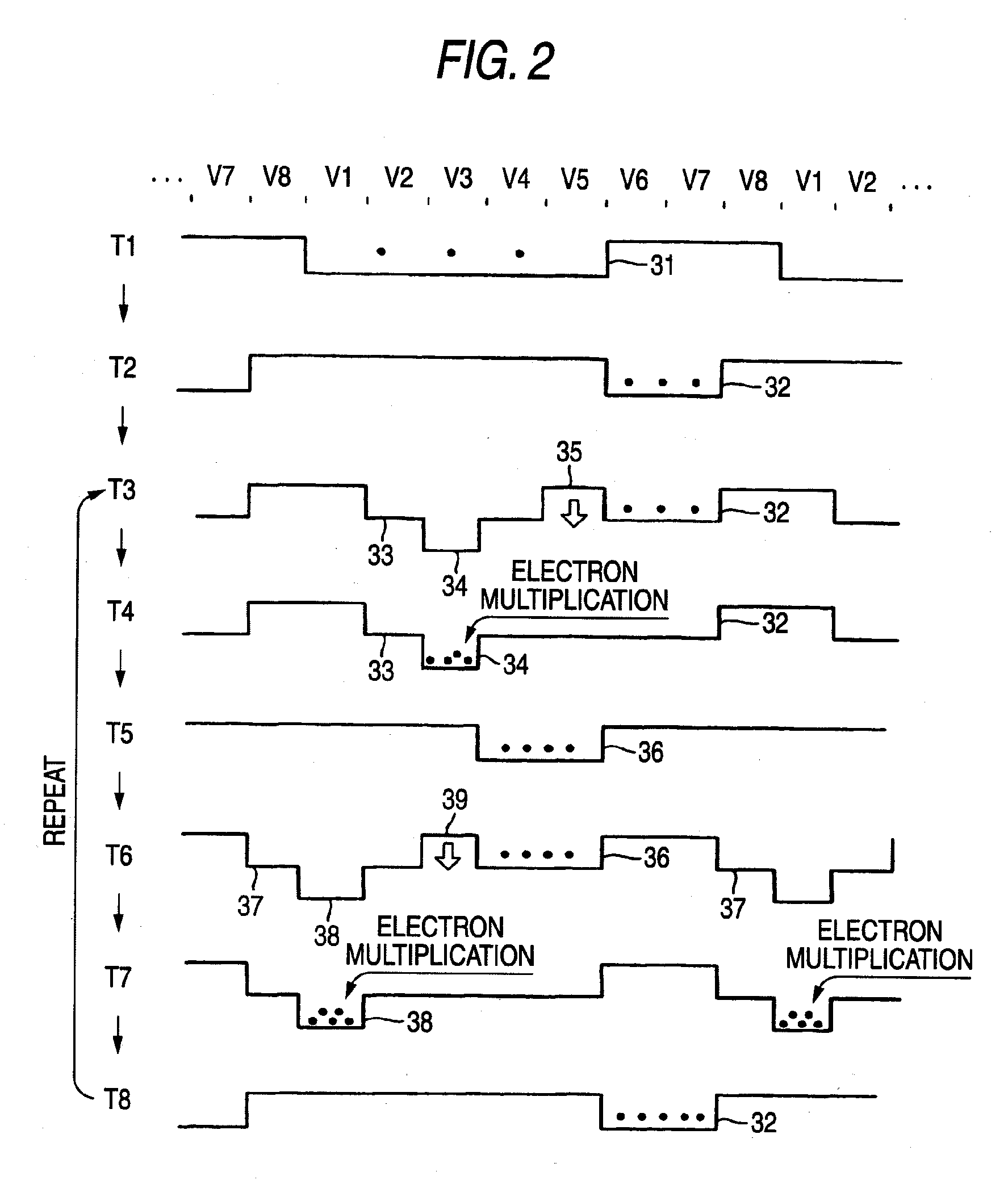
[0114]FIG. 7 is a view illustrating a method of driving a CCD solid-state image pickup device of a third embodiment of the invention. Similarly with the read pulse (TG) which is used for reading signal charges from pixels to the vertical charge transfer path, an electron multiplying pulse of high voltage is produced as a binary pulse voltage of, for example, 0 V (VM) and +15 V (VH).

[0115]When rising and falling edges of the electron multiplying pulse are steep (approximately vertical), however, the potential of a transfer electrode to which the electron multiplying pulse is applied is steeply changed, and an electric field applied to the transfer electrode and its vicinity is largely changed, thereby producing a possibility that the electrode and a semiconductor portion in the vicinity may be electrostatically broken. Moreover, the electron multiplying pulse is repeatedly applied many times. Even when electrostatic breakdown does not occur, therefore, the physical properties of the ...


PUM


Abstract

A method of driving a CCD solid-state image pickup device, which performs multiplication driving on the signal charges, the method including: reading out signal charges from a plurality of photoelectric converting elements that are arranged in a two-dimensional array-like pattern to a charge transfer path that is disposed in parallel to a photoelectric converting element column of the photoelectric converting elements; and applying a multiplying pulse to a multiplying electrode among transfer electrodes constituting the charge transfer path, wherein an electrode, which is set as the multiplying electrode among the transfer electrodes, is periodically changed.

Description

BACKGROUND OF THE INVENTION [0001]1. Field of the Invention[0002]The present invention relates to a method of driving a CCD (Charge Coupled Device) solid-state image pickup device which performs multiplication driving on signal charges, and also to an image pickup apparatus.[0003]2. Background Art[0004]FIG. 21 is a diagram illustrating a CCD solid-state image pickup device. FIG. 21A shows a solid-state image pickup device of a so-called honeycomb pixel arrangement in which the arrangement of even-row pixels (photoelectric converting elements (photodiodes: PDs)) 12 formed in a surface portion of a semiconductor substrate is staggered by ½ pitch from that of odd-row pixels, and FIG. 21B shows a solid-state image pickup device in which pixels are arranged in a square lattice pattern.[0005]A vertical charge transfer path (VCCD) 11 is disposed adjacent to each pixel column. A horizontal charge transfer path (HCCD) 13 is disposed along end portions of the vertical charge transfer paths 11...

Claims


Application Information

Patent Timeline
IPC IPC(8): H04N5/335H04N1/028H04N5/365H04N5/372
CPCH04N3/1537H04N3/1568H04N5/3728H04N25/441H04N25/709H04N25/73
Inventor KUSUDA, DAISUKEKOBAYASHI, HIROKAZUODA, KAZUYA
Owner FUJIFILM CORP
Why Eureka
Try Eureka