Method for manufacturing semiconductor device

a manufacturing method and semiconductor technology, applied in semiconductor devices, semiconductor/solid-state device details, printed circuits, etc., can solve the problems of short communication distance, small antenna size, poor connection, etc., and achieve the effects of preventing partial stretching of semiconductor devices, reducing manufacturing costs, and reducing manufacturing costs

Inactive Publication Date: 2008-12-18
SEMICON ENERGY LAB CO LTD
View PDF36 Cites 37 Cited by
  • Summary
  • Abstract
  • Description
  • Claims
  • Application Information

AI Technical Summary

Benefits of technology

[0007]In view of the above, the present invention provides a method for manufacturing a highly-reliable semiconductor device, which is not damaged by external local pressure, with a high yield.
[0013]Using high-strength fiber as the fibrous body, even when local pressure is applied to a semiconductor device, the pressure is dispersed throughout the fibrous body; accordingly, partial stretching of the semiconductor device can be prevented. That is, destruction of a wiring, a semiconductor element, or the like which is caused by partial stretching thereof, can be prevented.
[0014]In accordance with the present invention, a highly-reliable semiconductor device which is not easily damaged by external local pressure can be manufactured with high yield.

Problems solved by technology

However, in the case of a semiconductor device with a built-in (on-chip) antenna which is incorporated in a chip, the size of the antenna is small when the area occupied by the chip is small, leading to a problem of a short communication distance.
In the case where a semiconductor device is manufactured such that an antenna provided on a paper or a film medium is connected to a chip, poor connection is made and yield is reduced when the size of the chip is small.

Method used


Image

  • Method for manufacturing semiconductor device
  • Method for manufacturing semiconductor device
  • Method for manufacturing semiconductor device

Examples


embodiment mode 1

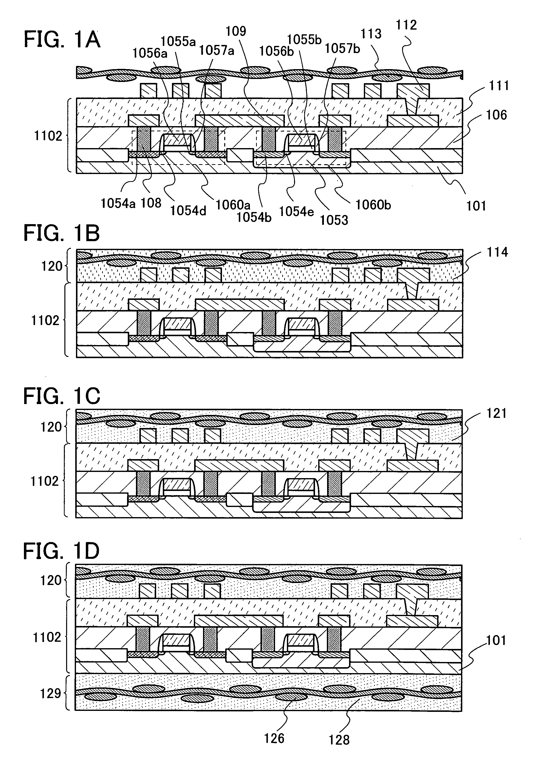
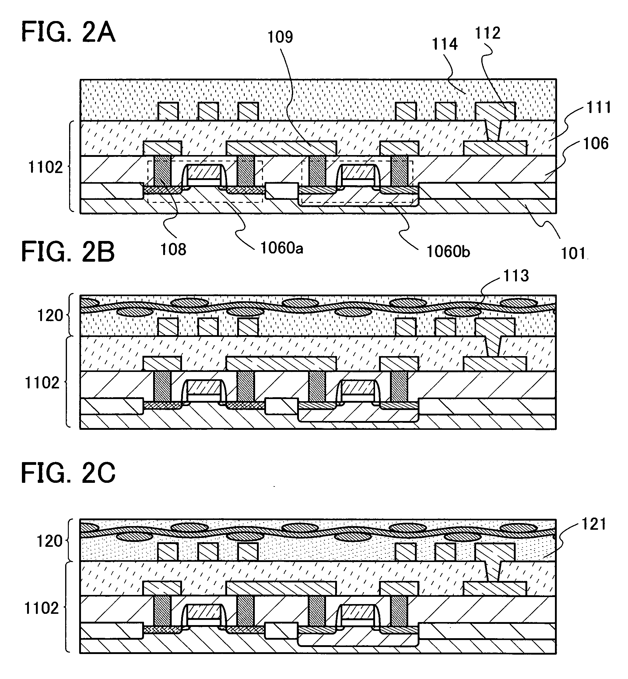
[0031]In this embodiment mode, a method of manufacturing a semiconductor device which is not easily damaged by external local pressure with high yield will be described with reference to FIGS. 1A to 1D.

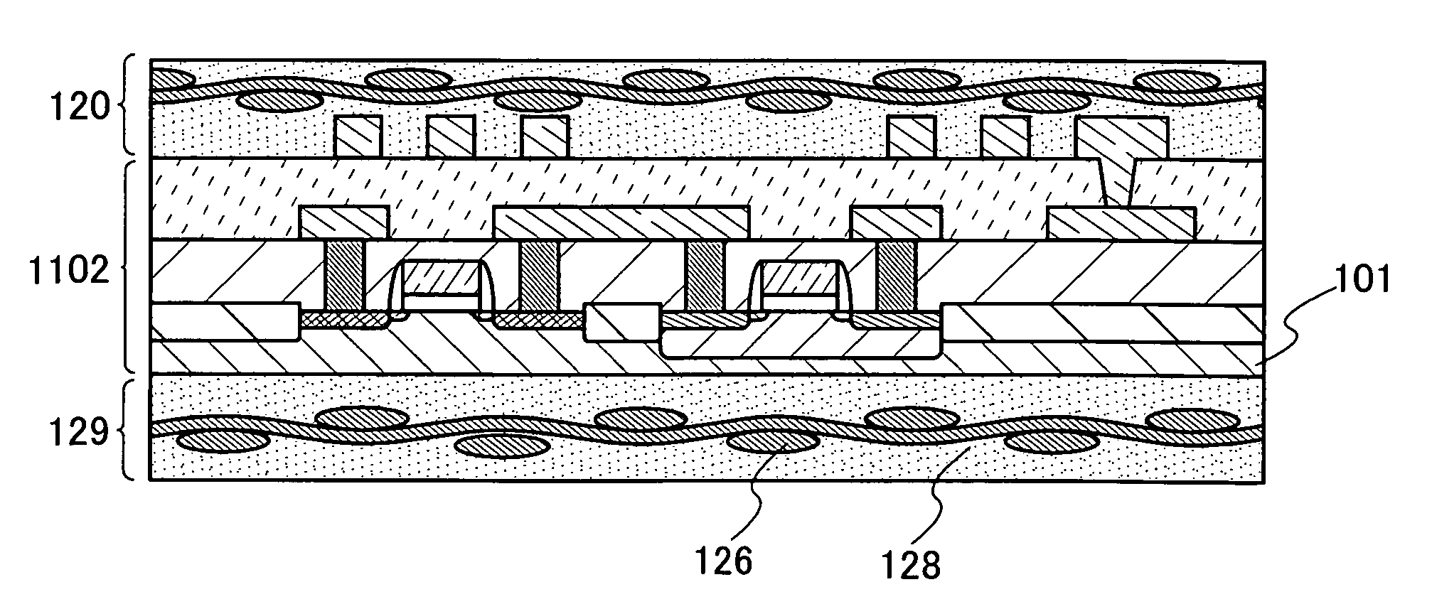
[0032]As shown in FIG. 1A, an antenna 112 and an element substrate 1102 having a semiconductor element formed using a single-crystal semiconductor substrate or an SOI substrate are formed. Next, a fibrous body 113 is provided over the element substrate 1102 and the antenna 112.

[0033]As typical examples of a semiconductor element included in the semiconductor substrate 1102, an active element such as a MOS transistor, a diode, or a nonvolatile memory element, and a passive element such as a resistor element or a capacitor element can be given. As a single-crystal semiconductor substrate, a single-crystal silicon substrate having n-type or p-type conductivity (a silicon wafer), or a compound semiconductor substrate (e.g., a GaAs substrate, an InP substrate, a GaN substrate, an SiC subst...

embodiment mode 2

[0091]In this embodiment mode, a manufacturing method of a semiconductor device which is not easily destroyed as compared with the one in Embodiment Mode 1, with reference to FIGS. 4A to 4C.

[0092]In a similar manner to Embodiment Mode 1, as shown in FIG. 4A, an antenna 112 and an element substrate 1102 including a semiconductor element formed using a single-crystal semiconductor substrate or an SOI substrate are formed. Then, a fibrous body 113 is provided over the element substrate 1102 and the antenna 112, an organic resin layer 114 is formed, and a protective film 131 is provided over the organic resin layer 114.

[0093]The protective film 131 is preferably formed from a high-strength material. As typical examples of a high-strength material, a polyvinyl alcohol resin, a polyester resin, a polyamide resin, a polyethylene resin, an aramid resin, a polyparaphenylene benzobisoxazole resin, a glass resin, and the like can be given.

[0094]Since the protective film 131 is formed from a hi...

embodiment mode 3

[0102]In this embodiment mode, a method for manufacturing a semiconductor device in which an antenna is not formed in an element substrate and an antenna provided over another substrate is connected to the element substrate will be described with reference to FIG. 5A to FIG. 7C.

[0103]As shown in FIG. 5A, a fibrous body 113 and an organic resin layer 155 having an opening 154 are formed over an element substrate 1151.

[0104]Here, as the element substrate 1151, as described in Embodiment Mode 1, the semiconductor substrate 101 is provided with the MOS transistors 1060a and 1060b. An insulating layer 106 is formed over the MOS transistors 1060a and 1060b, and conductive layers 108 and 109 which connect to a source region and a drain region of the MOS transistors are formed through the insulating layer 106. An insulating layer 111 is formed over the conductive layers 108 and 109 and the insulating layer 106, and an electrode pad 152 is formed so as to connect to the conductive layer 109 ...


PUM

PropertyMeasurementUnit
sizeaaaaaaaaaa
thicknessaaaaaaaaaa
thicknessaaaaaaaaaa

Abstract

To provide a method for manufacturing a highly-reliable semiconductor device, which is not damaged by external local pressure, with a high yield, a semiconductor device is manufactured by forming an element substrate having a semiconductor element formed using a single-crystal semiconductor substrate or an SOI substrate, providing the element substrate with a fibrous body formed from an organic compound or an inorganic compound, applying a composition containing an organic resin to the element substrate and the fibrous body so that the fibrous body is impregnated with the organic resin, and heating to provide the element substrate with a sealing layer in which the fibrous body formed from an organic compound or an inorganic compound is contained.

Description

BACKGROUND OF THE INVENTION[0001]1. Field of the Invention[0002]The present invention relates to a method for manufacturing a semiconductor device having a semiconductor element formed using a single-crystal semiconductor substrate or an SOI substrate.[0003]2. Description of the Related Art[0004]Currently, it is important to make various devices, such as wireless chips and sensors, into a thinner shape in miniaturizing products, and the technique and the application range spread rapidly. Such various devices which are made thin are flexible to some extent and thus the devices can be provided for an object having a curved surface.[0005]In Reference 1 (Japanese Published Patent Application No. 2004-78991), a semiconductor device is disclosed in which, a semiconductor chip with the size of less than or equal to 0.5 mm is embedded in paper or a film-like medium, so that tolerance for bending and concentrated loading is improved.SUMMARY OF THE INVENTION[0006]However, in the case of a sem...

Claims


Application Information

Patent Timeline
Patent Type & Authority Applications(United States)
IPC IPC(8): H01L21/56
CPCH01L23/293H01L27/12H01L27/1214H01L2924/12044H05K1/185H01L2924/0002H05K1/189H01L2924/00H01L21/20
Inventor DOZEN, YOSHITAKASUGIYAMA, EIJIOHTANI, HISASHITSURUME, TAKUYA
Owner SEMICON ENERGY LAB CO LTD
Why Eureka
Try Eureka