Low on-resistance lateral double-diffused mos device and method of fabricating the same

Active Publication Date: 2008-12-25
MACRONIX INT CO LTD
View PDF16 Cites 17 Cited by
  • Summary
  • Abstract
  • Description
  • Claims
  • Application Information

AI Technical Summary

Benefits of technology

[0006]The present invention is directed to a lateral double-diffused metal oxide semiconductor (LDMOS) device adapt

Problems solved by technology

When operating the LDMOS device, the gate dielectric layer is punched through by the hot electrons due to the high electric field and high currents in the drain termi

Method used


Image

  • Low on-resistance lateral double-diffused mos device and method of fabricating the same
  • Low on-resistance lateral double-diffused mos device and method of fabricating the same
  • Low on-resistance lateral double-diffused mos device and method of fabricating the same

Examples


Embodiment Construction

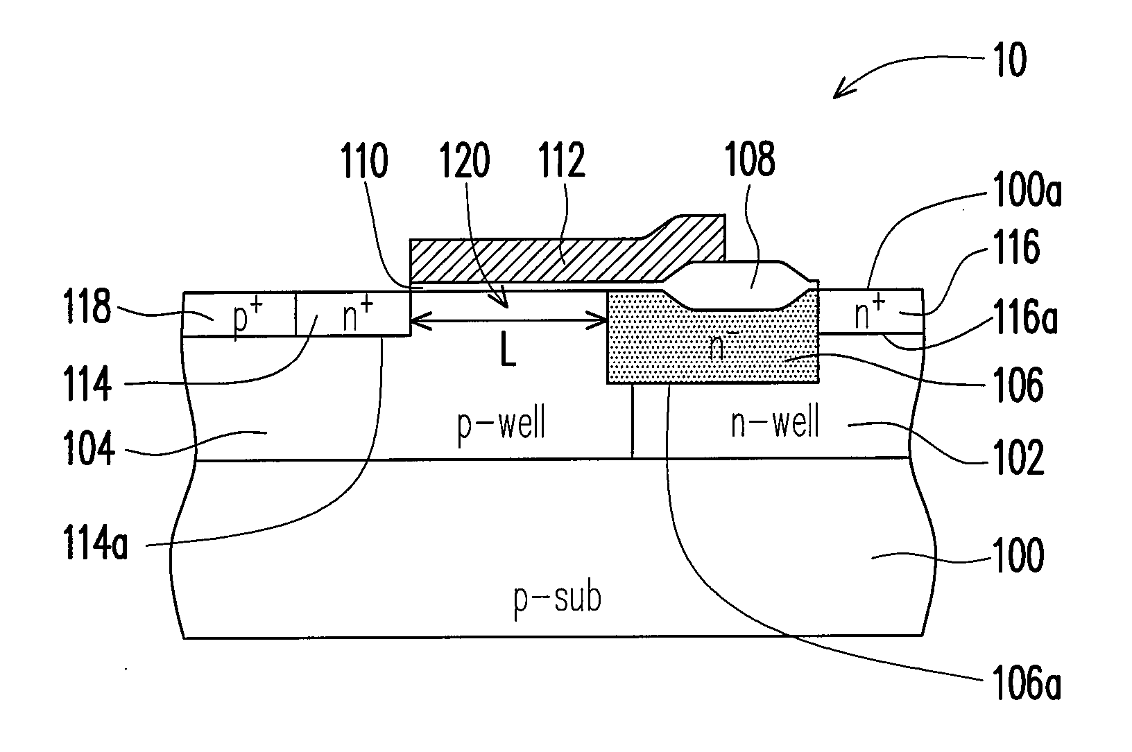
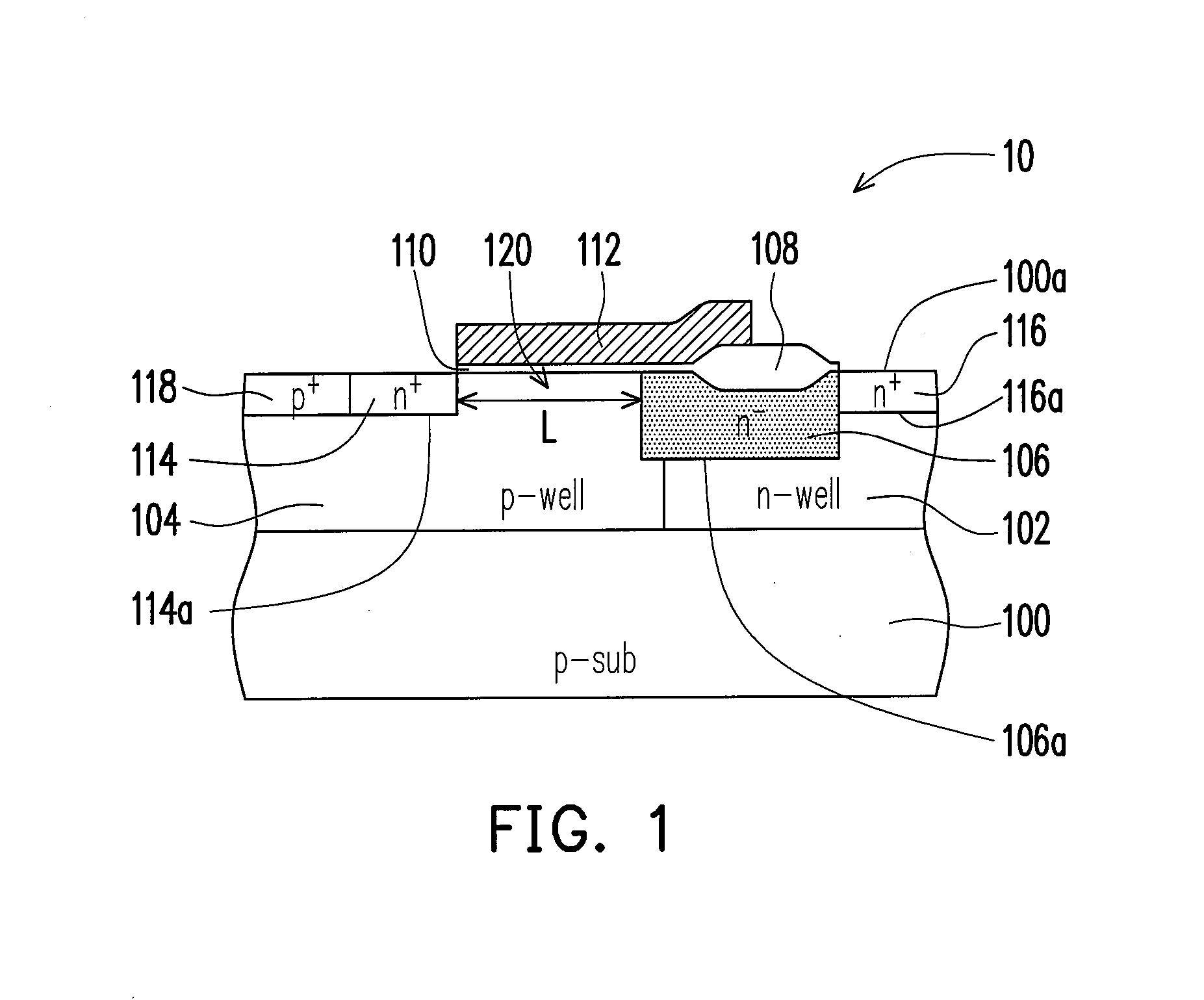
[0030]Referring to FIG. 1, a lateral double-diffused metal oxide semiconductor (LDMOS) device 10 includes a first well 102 having a first conductive type such as n-type, a second well 104 having a second conductive type such as p-type, an third doped region 106 having the first conductive type such as n-type, a field oxide layer 108, an first doped region 116 having the first conductive type such as n-type as a drain region, an second doped region 114 having the first conductive type such as n-type as a source region, a gate dielectric layer 110, a gate conductive layer 112 and a bulk contact region 118 having the second conductive type such as p-type.

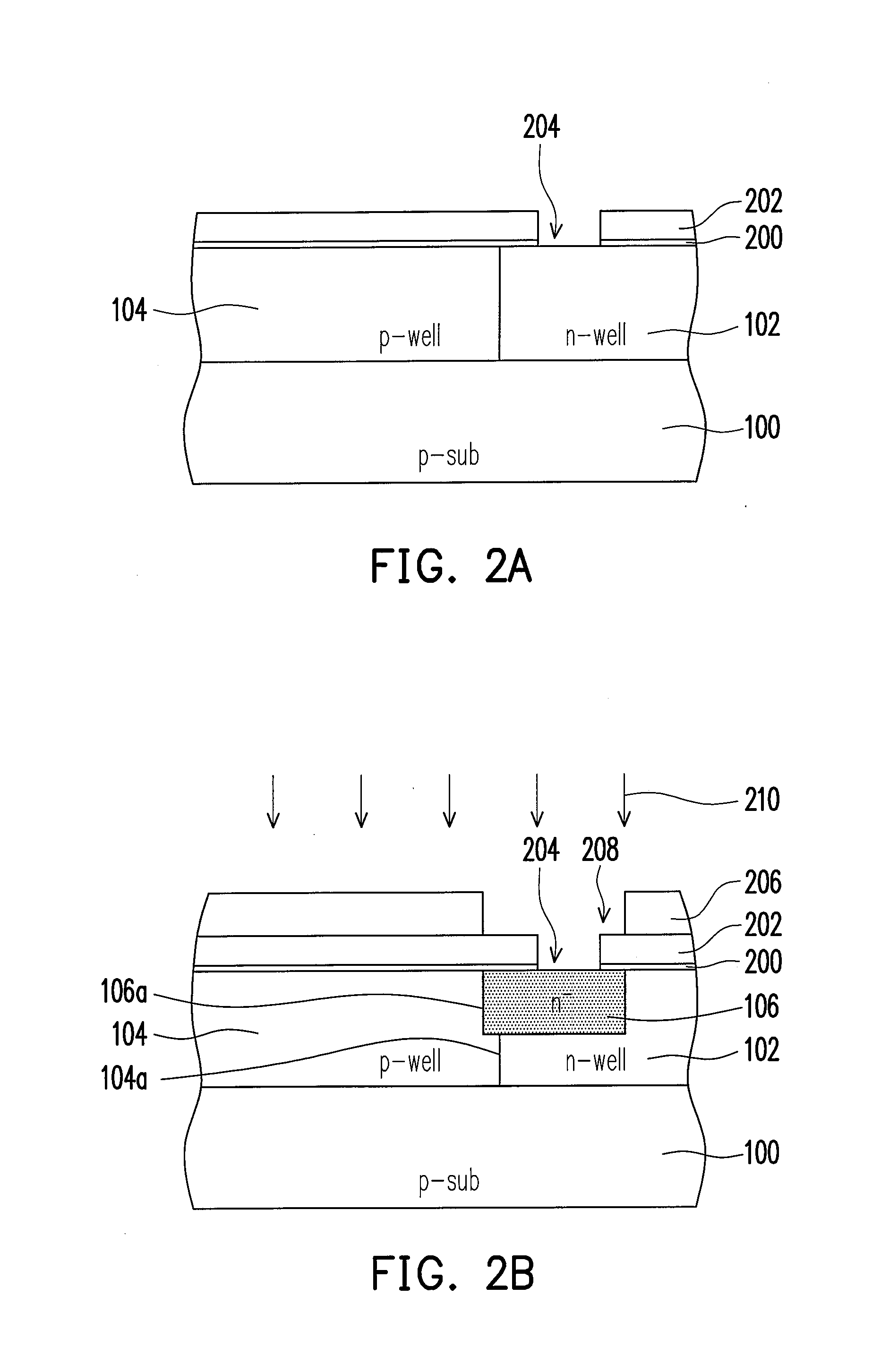
[0031]The first well 102 and the second well 104 are disposed in a substrate 100 and are adjacent to each other. The method used for fabricating the first well 102 and the second well 104 is respectively forming a photoresist pattern using an ion implantation process and a drive-in process.

[0032]The source region 114 is disposed in the...


PUM


Abstract

A lateral-double diffused MOS device is provided. The device includes: a first well having a first conductive type and a second well having a second conductive type disposed in a substrate and adjacent to each other; a drain and a source regions having the first conductive type disposed in the first and the second wells, respectively; a field oxide layer (FOX) disposed on the first well between the source and the drain regions; a gate conductive layer disposed over the second well between the source and the drain regions extending to the FOX; a gate dielectric layer between the substrate and the gate conductive layer; a doped region having the first conductive type in the first well below a portion of the gate conductive layer and the FOX connecting to the drain region. A channel region is defined in the second well between the doped region and the source region.

Description

BACKGROUND OF THE INVENTION[0001]1. Field of the Invention[0002]The present invention relates to an integrated circuit and a method of fabricating the same, and more particularly, to a lateral double-diffused metal oxide semiconductor (LDMOS) device and a method of fabricating the same.[0003]2. Description of Related Art[0004]A lateral double-diffused metal oxide semiconductor (LDMOS) device is a typical high voltage device and the process of fabricating the same can be integrated with the process of fabricating complementary metal oxide semiconductor (CMOS) to fabricate control, logic and power switches on a single chip. When operating a LDMOS device, a high breakdown voltage and a low on-state resistance (Ron) must be provided. The LDMOS device with a high breakdown voltage and a low on-state resistance (Ron) has a comparatively lower power consumption when being operated under high voltage. Further, a lower on-state resistance (Ron) allows a higher drain current when the transist...

Claims


Application Information

Patent Timeline
IPC IPC(8): H01L29/78H01L21/336
CPCH01L29/0847H01L29/42368H01L29/66659H01L29/7835
Inventor HUANG, HSUEH-ICHU, CHIEN-WENLIN, CHENG-CHILIEN, SHIH-CHINYEH, CHIN-PENWU, SHYI-YUAN
Owner MACRONIX INT CO LTD
Why Eureka
Try Eureka