Sensing circuit, optical detection circuit, display device, and electronic apparatus

a technology of optical detection and sensing circuit, applied in the direction of optical radiation measurement, identification means, instruments, etc., can solve the problem that the deviation of a detected luminance caused by photodegradation cannot be corrected, and achieve the effect of accurately correcting the deviation of a detection valu

Active Publication Date: 2008-12-25
BOE TECH GRP CO LTD
View PDF2 Cites 3 Cited by
  • Summary
  • Abstract
  • Description
  • Claims
  • Application Information

AI Technical Summary

Benefits of technology

[0009]An advantage of some aspects of the invention is to provide a sensing circuit and an optical detection circuit capable of accurately correcting a deviation of a detection value caused by temporal degradation of a sensing element by using two sensing elements having the same sensing characteristic and a display device and an electronic apparatus using the same. In addition, another advantage of some aspects of the invention is to make it possible to correct a deviation of a detection value caused by temporal degradation of a sensing element by using two sensing elements having the same sensing characteristic even in cases of sensors other than an image sensor.
[0012]Furthermore, in the sensing circuit described above, the detection unit may detect the size of the energy on the basis of the second rate of degradation specified by the specifying unit, the second output signal, and the predetermined reduction rate instead of detecting the size of the energy on the basis of the first rate of degradation specified by the specifying unit and the first output signal. Even in this configuration, an accurate detection value can be obtained.
[0015]Furthermore, in the sensing circuit described above, the storage unit may store as the degradation characteristic the relationship between a second rate of degradation, which indicates a degree of degradation of the input and output characteristics of the second sensing element, and the output ratio, which is a ratio between the level of the first output signal and the level of the second output signal, instead of storing as the degradation characteristic the relationship between the first rate of degradation, which indicates the degree of degradation of the input and output characteristics of the first sensing element, and the output ratio that is a ratio between the level of the first output signal and the level of the second output signal. The specifying unit may calculate the ratio between the level of the first output signal and the level of the second output signal, compare the calculated ratio with the output ratio of the degradation characteristic obtained by referring to the storage unit, and specify the second rate of degradation on the basis of a result of the comparison instead of calculating the ratio between the level of the first output signal and the level of the second output signal, comparing the calculated ratio with the output ratio of the degradation characteristic obtained by referring to the storage unit, and specifying the first rate of degradation on the basis of a result of the comparison. The detection unit may detect the size of the energy on the basis of the second rate of degradation specified by the specifying unit, the second output signal, and the predetermined reduction rate instead of detecting the size of the energy on the basis of the first rate of degradation specified by the specifying unit and the first output signal. Even in this configuration, an accurate detection value can be obtained.
[0021]Furthermore, in the optical detection circuit described above, the storage unit may store the relationship between a rate of degradation, which indicates a degree of degradation of efficiency of photoelectric conversion in the second photoelectric conversion element, and the output ratio indicating a ratio between the level of the first output signal and the level of the second output signal instead of storing the relationship between the rate of degradation, which indicates the degree of degradation of efficiency of photoelectric conversion in the first photoelectric conversion element, and the output ratio indicating a ratio between the level of the first output signal and the level of the second output signal. The calculation unit may calculate the luminance of incident light on the basis of the specified rate of degradation, the second output signal, and the predetermined light reduction rate instead of calculating the luminance of incident light on the basis of the specified rate of degradation and the first output signal. Even in this configuration, an accurate detection luminance can be obtained.

Problems solved by technology

In such an optical sensor, a deviation of a detected luminance caused by photodegradation cannot be corrected even if the same environmental light is incident on two photoelectric conversion elements having the same photoelectric conversion characteristics.

Method used


Image

  • Sensing circuit, optical detection circuit, display device, and electronic apparatus
  • Sensing circuit, optical detection circuit, display device, and electronic apparatus
  • Sensing circuit, optical detection circuit, display device, and electronic apparatus

Examples


first embodiment

1. First Embodiment

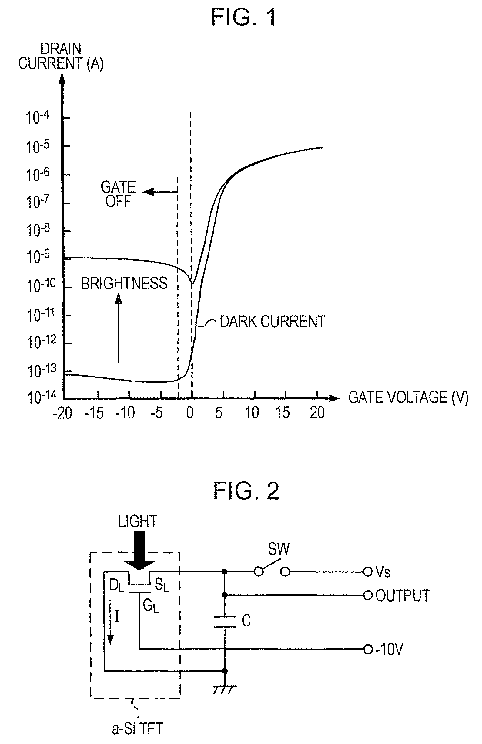
[0045]FIG. 1 is a graph illustrating the relationship between a gate voltage and a drain current of an a-Si TFT (amorphous silicon TFT: amorphous silicon thin film transistor) used as a photoelectric conversion element. Noting a period of time for which a gate is in an OFF state, in the case when light does not be incident on a channel portion, only a leak current (drain current) of 10−13 A or less flows as shown as a dark current in the drawing. In contrast, in the case when light is incident on the channel portion during the same period of time for which the gate is in the OFF state, a leak current corresponding to the intensity (brightness) of the light that is incident on the channel portion flows. That is, in the case of the a-Si TFT, the intensity of a leak current during a period of time for which the gate is in the OFF state is proportional to the intensity of light that is incident on the channel portion.

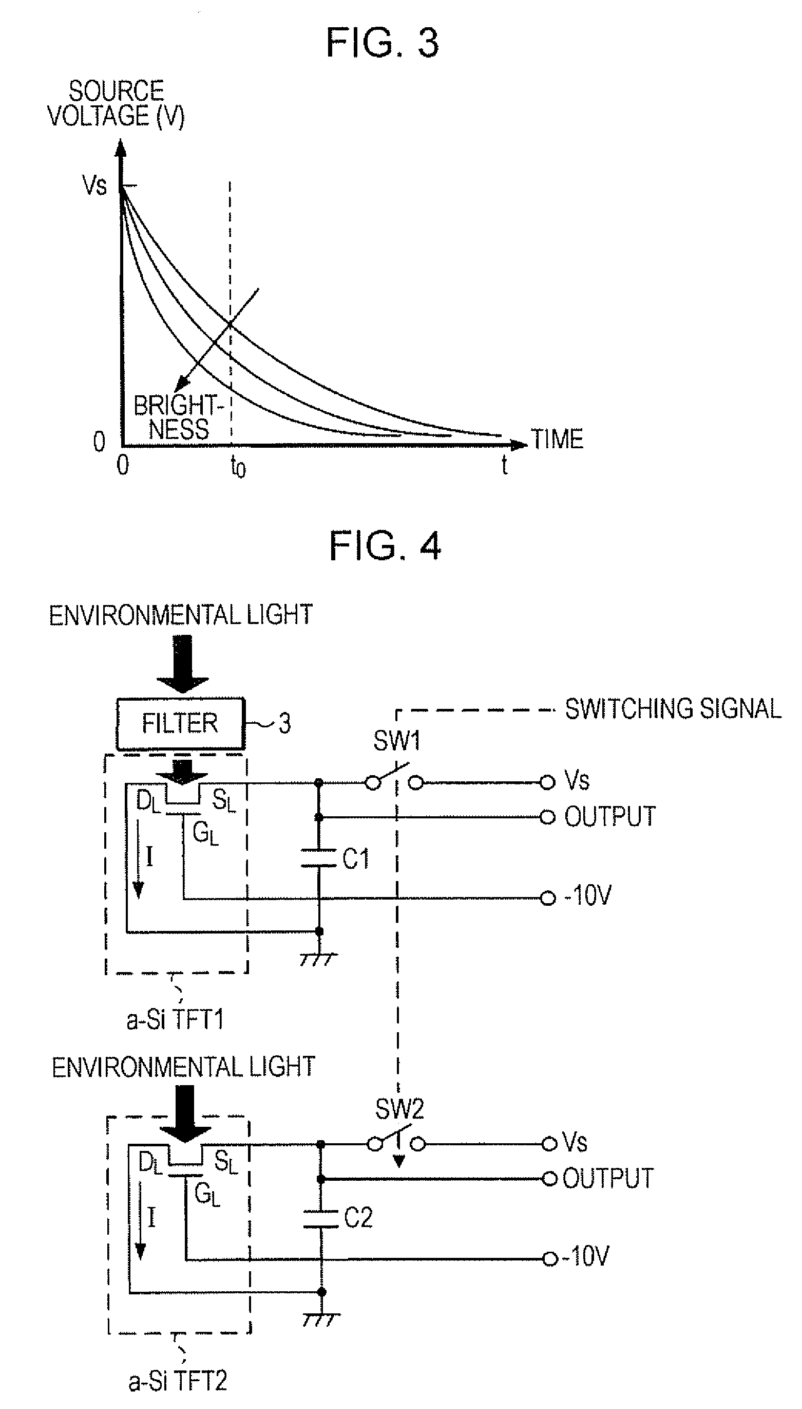
[0046]It is preferable to use a circuit shown in FI...

second embodiment

2. Second Embodiment

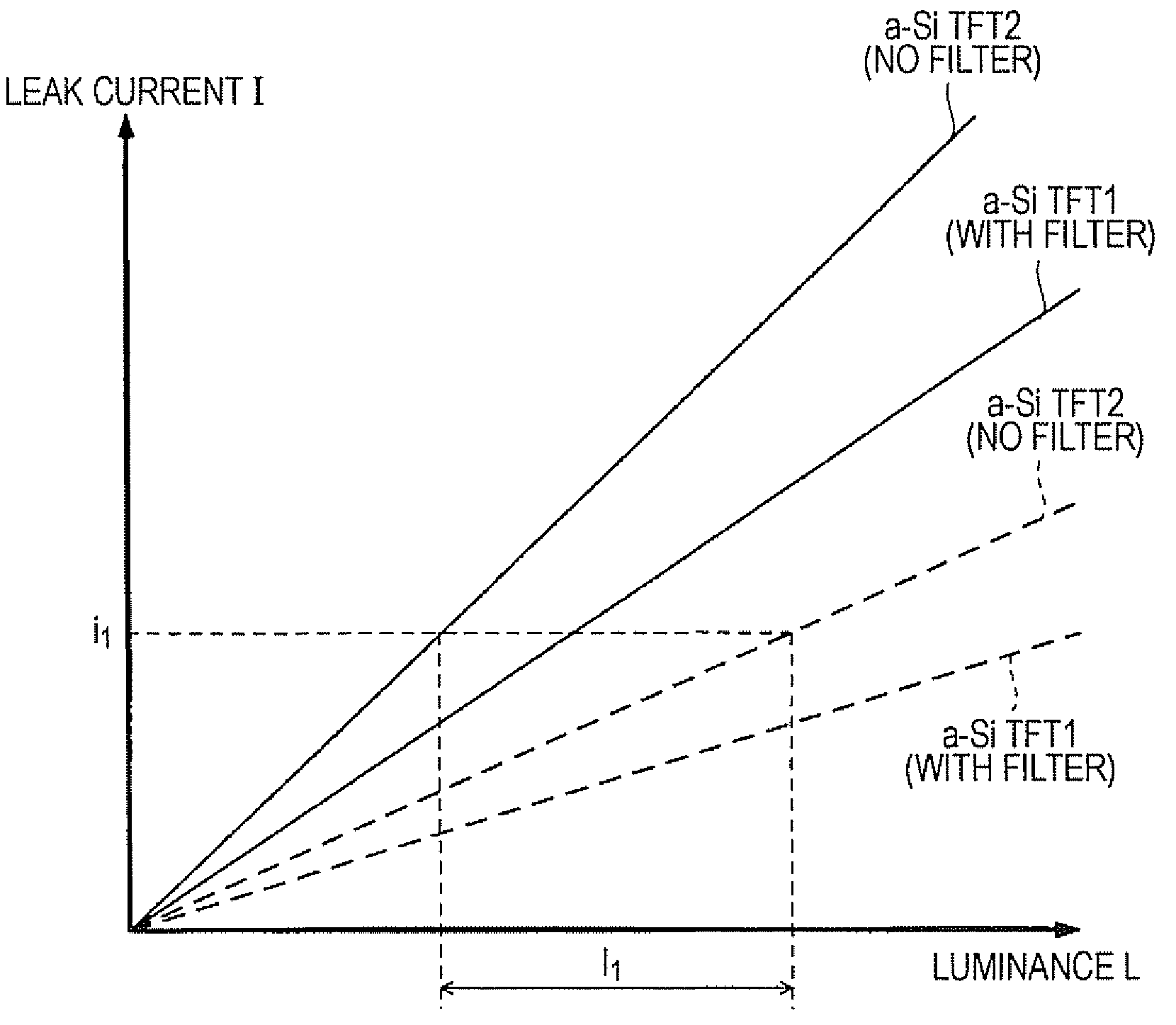
[0074]The case in which the dark filter having a transmittance of 10% is used as the filter 3 has been described in the first embodiment, while a case in which a green color filter is used as the filter 3 will be described in the present embodiment. Moreover, in the present embodiment, the same constituent elements as in the first embodiment are denoted by the same reference numerals, and an explanation thereof will be omitted.

[0075]An optical sensor circuit in the present embodiment includes the circuit shown in FIG. 4, in the same manner as that in the first embodiment. However, the second embodiment is different from the first embodiment in that a green color filter is used as the filter 3 and the incident light amount of the a-Si TFT1 is smaller than that of the a-Si TFT2 due to the green color filter. In the case where a green color filter is used as the filter 3 as described above, the relationship between an integrated luminance and a leak current in an a-...

third embodiment

3. Third Embodiment

[0091]In the present embodiment, a display device that adjusts the brightness of the entire screen according to the luminance (ambient brightness) of environmental light by using the optical sensor circuit 5 and the optical detection circuit 10 described in the first embodiment or the optical sensor circuit 15 and the optical detection circuit 20 described in the second embodiment will be described.

[0092]FIG. 16 is a block diagram illustrating the configuration of a display device 50 according to the present embodiment. The display device 50 is a transmissive liquid crystal display device and includes a liquid crystal panel AA, an optical detection circuit 350, a light control circuit 400, a backlight 500, a control circuit 600, and an image processing circuit 700. In addition, an image display region A, a scanning line driving circuit 100, a data line driving circuit 200, and an optical sensor circuit 300 are provided in the liquid crystal panel AA. In the image ...


PUM

PropertyMeasurementUnit
reflectanceaaaaaaaaaa
drain currentaaaaaaaaaa
gate voltageaaaaaaaaaa

Abstract

A sensing circuit includes a first sensing element, a second sensing element, a reduction unit, a storage unit, a specifying unit and a detection unit. The reduction unit reduces the amount of the energy applied to the second sensing element. The storage unit stores a degradation characteristic of the sensing element. The specifying unit specifies a rate of degradation. The detection unit detects the amount of the energy on the basis of the rate of degradation.

Description

BACKGROUND[0001]1. Technical Field[0002]The present invention relates to a sensing circuit and an optical detection circuit capable of detecting a luminance, a temperature, and the like, and a display device and an electronic apparatus using the same.[0003]2. Related Art[0004]In an optical sensor that uses an amorphous silicon thin film transistor as a photoelectric conversion element, a difference between a detected luminance and a true luminance gradually increases with time. This is because the phenomenon of photodegradation that the conductivity decreases with increasing integrated luminance occurs. In order to eliminate a deviation of the detected luminance caused by such photodegradation, for example, JP-A-6-350803 discloses using two equal photoelectric conversion elements.[0005]Specifically, JP-A-6-350803 discloses a line image sensor in which photoelectric conversion elements 1 and 2, which have almost the same structure as a thin film transistor used in an active-matrix-dr...

Claims


Application Information

Patent Timeline
Patent Type & Authority Applications(United States)
IPC IPC(8): G01J1/10G01D3/028G01J1/42G01J1/44G01K7/00G09F9/00G09G3/20G09G5/00
CPCG01J1/02G01J1/0228G01J1/0238G01J1/46G01D3/028G01J1/42G01K7/00G09G3/20
Inventor ISHII, RYOSATO, TAKASHIKUNIMORI, TAKASHI
Owner BOE TECH GRP CO LTD
Why Eureka
Try Eureka