Electrochemical deposition platform for nanostructure fabrication

a nano- and micro-sized technology, applied in the direction of mechanical roughness/irregularity measurement, machining electric circuits, instruments, etc., can solve the problems of electrolyte bath-based deposition not being suitable for devices, porous structure produced by this method,

Inactive Publication Date: 2009-01-01
THE BOARD OF TRUSTEES OF THE UNIV OF ILLINOIS
View PDF2 Cites 32 Cited by
  • Summary
  • Abstract
  • Description
  • Claims
  • Application Information

AI Technical Summary

Benefits of technology

[0023]e. increasing the vertical separation between the reservoir and the substrate while maintaining an electrical current therebetween which is constant to within 15%, thereby forming a structure of the selected material which extends at least partially upwards from the surface of the substrate.

Problems solved by technology

However, structures produced by this method are usually porous and have feature sizes in the tens of micrometers (Said, ibid.) due to the limitation in producing and maintaining a sharp conductive probe and in confining the electric field down to nanoscale dimensions.
In addition, electrolyte bath-based deposition is not suitable for devices in which exposure to ionic solution needs to be avoided.

Method used


Image

  • Electrochemical deposition platform for nanostructure fabrication
  • Electrochemical deposition platform for nanostructure fabrication
  • Electrochemical deposition platform for nanostructure fabrication

Examples


example 1

Electrodeposition of Cu Nanowires

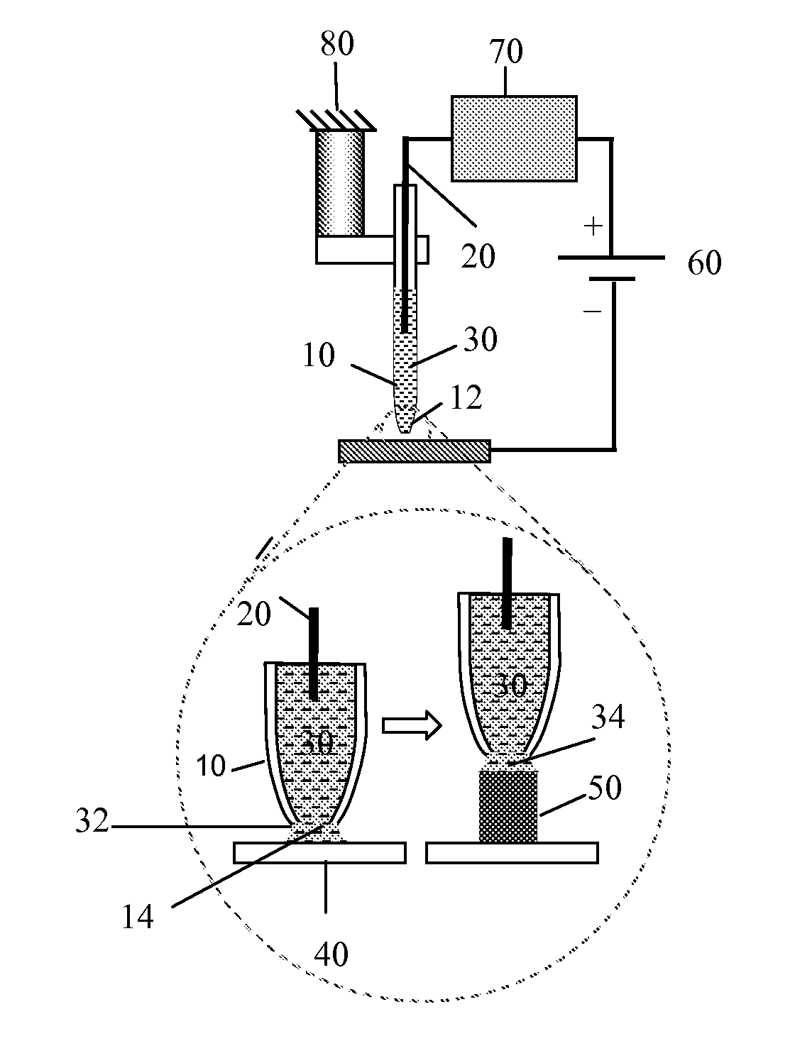
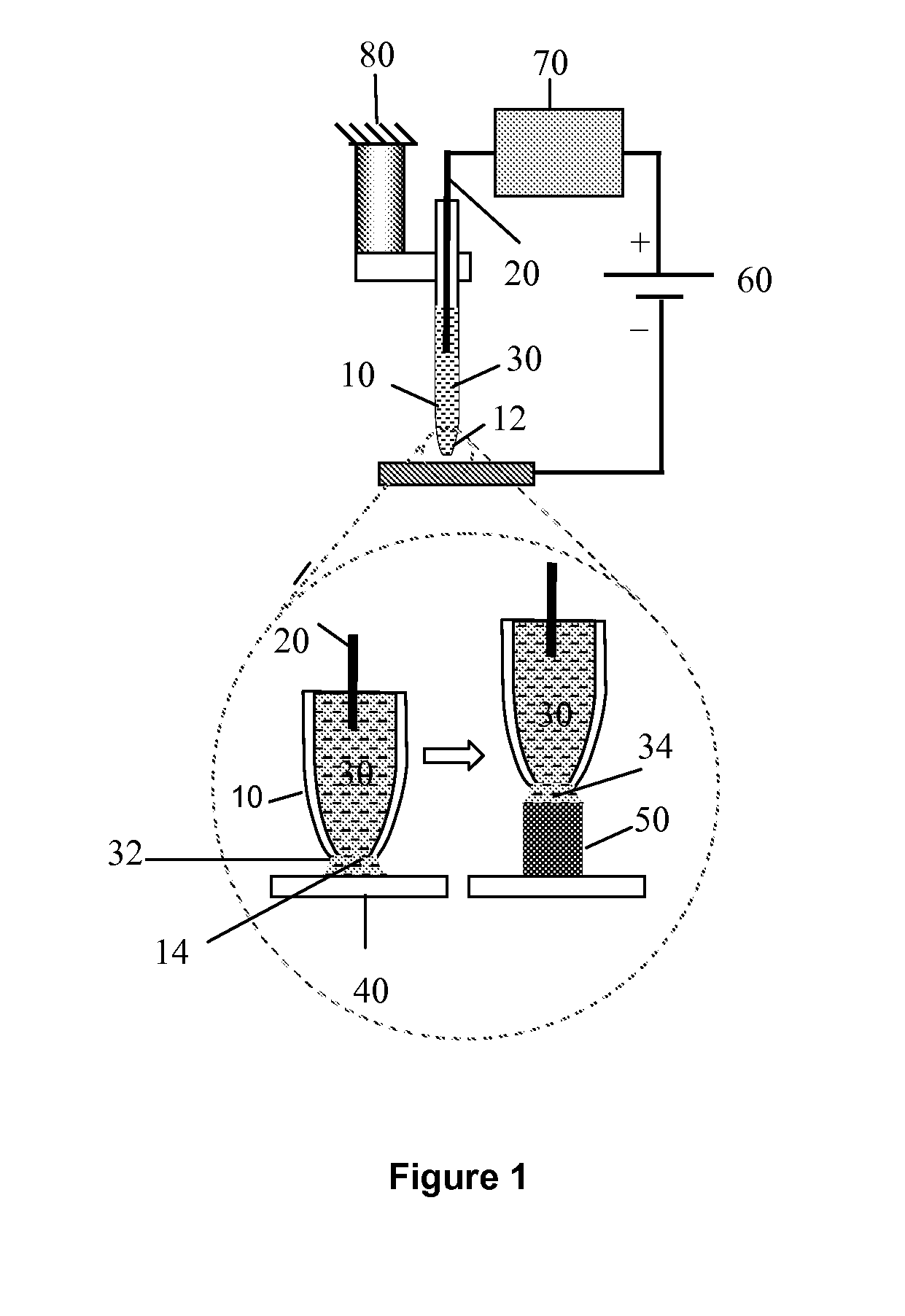
[0109]Commercially available glass pipets with aperture sizes of 500, 200, and 100 nm were used. The selected pipet was filled with 0.05 M CuSO4 electrolyte (Transene Inc.) and mounted on a custom made piezo-driven flexure stage which provided fine nanometer resolution linear motion. A Cu electric wire was inserted into the electrolyte inside the pipet and functioned as an anode. A silicon substrate coated with 5 nm / 100 nm thick chrome / gold film served as a cathode and the sample surface for the nanowire deposition. Coarse motions in the x, y, and z directions were provided by Burleigh inchworm stages. For the deposition, an electric potential was applied between the substrate and the copper wire inserted into the pipet, and the pipet was moved towards the substrate by the fine and coarse motion stages. The ionic current was measured with an electrometer and monitored by a control system. As soon as the pipet came in contact with the substrate, an el...

example 2

Electrodeposition of Pt Nanowires

[0115]Commercially available glass nanopipets with apertures as small as 100 nm were filled with 5 mM chloroplatinic acid (H2PtCl6) (pH=1) solution (Sigma-Aldrich Inc.) and used as electrochemical fountain pens. Platinum was chosen for deposition. A two-electrode configuration was used for the electrochemical deposition and the monitoring of electrochemical process (Bard, A. J. and Faulkner, L. R., “Electrochemical Methods: Fundamentals and Applications, 2nd Edition,” John Wiley & Sons, Inc, New York, 2001). A 250 μm diameter platinum wire was inserted into the nanopipet to act as the reference electrode during deposition. For convenience in later characterization, the cantilever surface of a conductive (Pt / Ir coated) AFM probe was used as the working electrode and the surface for nanowire deposition. The cantilever of the AFM probe, which has a relatively high spring constant of ˜3 N / m, acts just as a rigid substrate, and introduces no obvious uncer...

example 3

Electrodeposition of Microsized Metal Tubes

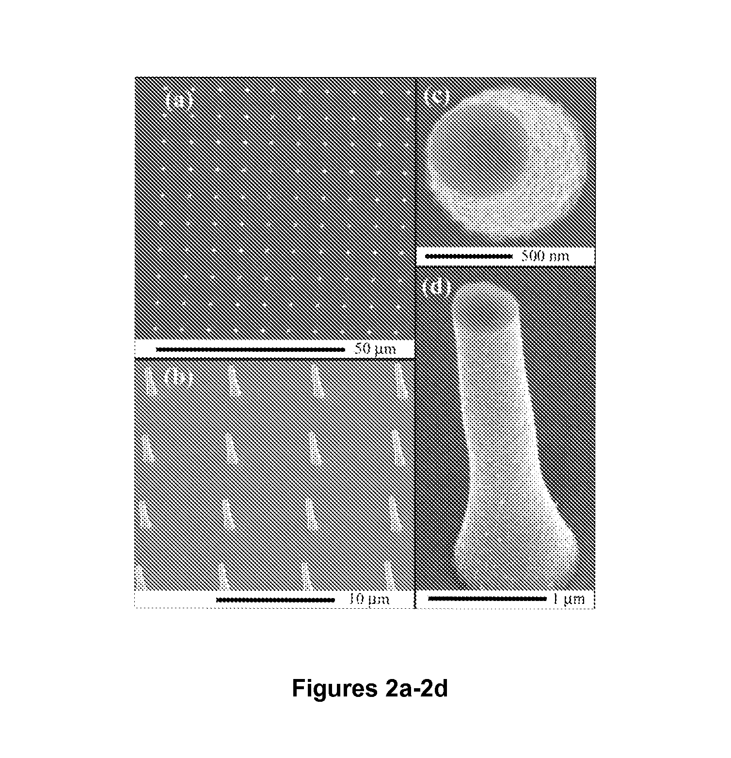
[0122]Microsized metal tubes have been deposited having an outer diameter of 2 microns and a wall thickness less than 0.5 nm. Experimental conditions were similar to those in Example 1, but the pipette had a larger aperture, approximately 2 microns. FIG. 8a shows an SEM image of the outside of the tube; FIG. 8b is a cutaway view of the tube in FIG. 8a.


PUM

PropertyMeasurementUnit
sizeaaaaaaaaaa
aspect ratioaaaaaaaaaa

Abstract

Probe-based methods are provided for formation of one or more nano-sized or micro-sized elongated structures such as wires or tubes. The structures extend at least partially upwards from the surface of a substrate, and may extend fully upward from the substrate surface. The structures are formed via a localized electrodeposition technique. The electrodeposition technique of the invention can also be used to make modified scanning probe microscopy probes having an elongated nanostructure at the tip or conductive nanoprobes. Apparatus suitable for use with the electrodeposition technique are also provided.

Description

CROSS-REFERENCE TO RELATED APPLICATIONS[0001]This application claims the benefit of U.S. Provisional Application 60 / 890,787, filed Feb. 20, 2007, which is hereby incorporated by reference to the extent not inconsistent with the disclosure herein.STATEMENT REGARDING FEDERALLY SPONSORED RESEARCH OR DEVELOPMENT[0002]This invention was made with government support under grant DMI-0328162 awarded by the National Science Foundation. The government has certain rights in the invention.BACKGROUND OF THE INVENTION[0003]This invention is in the field of electrochemical fabrication of nano and micro-sized structures, including metallic, semiconducting, and polymeric structures.[0004]Due to the versatility of electrochemistry for plating and surface finishing of a wide range of materials, the principle of electrochemistry has recently been pursued and applied for the fabrication of various metallic nanostructures.[0005]For example, electrochemical deposition has been used to deposit large arrays...

Claims


Application Information

Patent Timeline
Patent Type & Authority Applications(United States)
IPC IPC(8): G01B5/28C25D1/04C25B15/02
CPCC25D17/00C25D1/00C25D1/006C25D1/04C25D1/02
Inventor YU, MIN-FENG
Owner THE BOARD OF TRUSTEES OF THE UNIV OF ILLINOIS
Why Eureka
Try Eureka