Evaluation method for interconnects interacted with integrated-circuit manufacture

a technology of interconnections and evaluation methods, which is applied in the direction of error detection/correction, semiconductor/solid-state device testing/measurement, instruments, etc., can solve the problems of significant timing delay in circuits, non-uniformity of conductor wires and dielectric thicknesses, and product yield loss, so as to improve manufacturing yield and improve interconnect layout design

Inactive Publication Date: 2009-01-01
LINDEN DESIGN TECH
View PDF10 Cites 3 Cited by
  • Summary
  • Abstract
  • Description
  • Claims
  • Application Information

AI Technical Summary

Benefits of technology

[0016]The accurate and thorough evaluation on the reaction of the interconnect conductor wire layout to the IC manufacture processes in any location of any IC layouts by the above evaluation method effectively provides useful insights and feedbacks to layout designers to improve the interconnect layout design in products, which consequently improves the manufacturing yield.

Problems solved by technology

Consequently, increasingly smaller, more compact and more delicate features of the interconnect conductor wires are becoming essential to handle such formidable task in the design and manufacture of the ICs.
However, the smaller, more compact and more delicate interconnect conductor wire features are beginning to interact with the IC manufacturing processes, causing product yield loss.
The interaction between the interconnect conductor wire features and the planarization process of the interconnect conductor and dielectric layers such as, but not limited to, the chemical-mechanical polish (CMP) process, can cause non-uniformity of the conductor wire and dielectric thickness due to the dishing on the conductor wire surface and the erosion on the dielectric surface.
Such effect reduces thickness of the interconnect conductor and dielectric layers, thus increasing the conductor wire resistance and the dielectric capacitance which can cause significant timing delays in circuits.
Since there can be up to ten or more interconnect conductor and dielectric layers in the 65-nanometer technologies and beyond, the accumulated effect of the non-uniformity of the interconnect conductor wire and dielectric thickness can be formidable after all interconnect conductor and dielectric layers receive the planarization process.
The interaction between the interconnect conductor wire features and the lithography process can cause the conductor wires either short or open.
The interaction between the interconnect conductor wire features and the plasma-involved interconnect dielectric deposition and etch process or the plasma-involved interconnect conductor etch process can cause damage to transistor gate oxides via the plasma induced charging current.
Degradation of the transistor gate oxides by such effect has become one of the serious transistor reliability concerns in the industry.
To date, a thorough and complete understanding of such interaction has not been rendered yet, partly because a thorough and complete design covering the best possible scenarios of the interconnect conductor wire features in product circuits has not been realized.

Method used


Image

  • Evaluation method for interconnects interacted with integrated-circuit manufacture
  • Evaluation method for interconnects interacted with integrated-circuit manufacture
  • Evaluation method for interconnects interacted with integrated-circuit manufacture

Examples


illustration 300

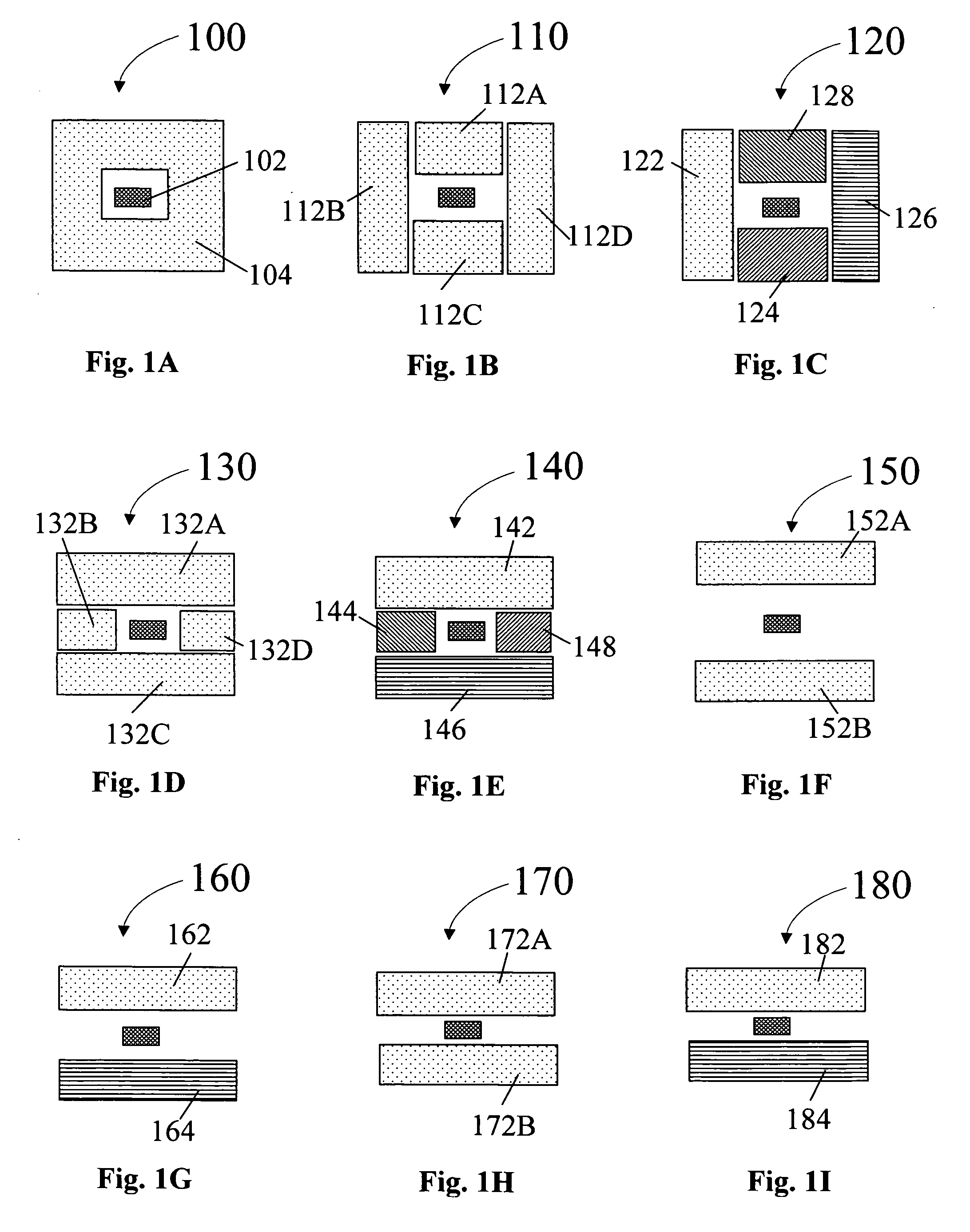
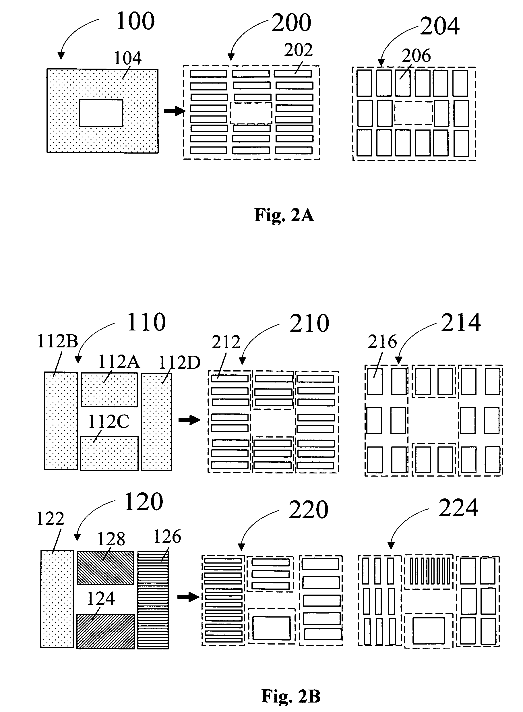
[0035]Illustration 300 in FIG. 3 shows layout examples of a Sensor 102 from a top view. Sensor 310, 320, 330, 340, 350, 360 and 370 show that they can be of any shape, size and orientation. In reality, they can be straight or curved, and not limited to a rectangular or square as shown in this figure. A Sensor can be a transistor, conductor, resistor, capacitor, inductor, etc., depending on where (at which layer) it is located in the silicon circuits. Note that the dotted-line region of the the transistor Sensor 370 illustrated in FIG. 3 is a diffusion or doped silicon layer, not a conductor layer.

(Method of Design)

[0036]The method of the design is to first identify an Environment that is the most basic type to construct the IC interconnect layouts. This can be achieved by investigating many existing IC layout designs to identify the most basic-element Environments. By varying or scaling the dimension of an identified basic-element Environment and by arranging the varied and scaled ...

illustration 400

[0037]Illustration 400 in FIG. 4 illustrates a general design method for interconnect test structures to accurately capture the response of the interaction between the interconnects and the IC manufacture processes. The simple Environment illustrated in Illustration 400 can be considered as a basic-element Environment constructing the IC layouts. It has two Fields, Field A (410) and Field B (420), side by side with a empty gap, a part of the empty Field C, in between. Fields A and B can have different or same interconnect conductor wire features within. In Illustration 400, the interconnect conductor wire features are different in Fields A and B. Field C is the total combined empty regions around Fields A and B. Field C has no interconnect conductor wires within. A Sensor 102 is placed at different locations of this basic-element Environment. In general, a typical IC layout is basically the repetition of such type of Environment with varied depth of Field A and Field B and of the Fi...

illustration 500

[0057]Illustration 500 in FIG. 5 is a specific example of the design method. The basic Environment element shown resembles the basic cases in IC layout design with Fields A and B comprising narrower rectangle-shaped wires. Three groups of variables are varied here. They are (1) the location of the Sensor 102; (2) the depth of Fields A and B, hA and hB, and the depth of Field-C gap region between Fields A and B, hC; (3) the interconnect conductor wire features such as the wire width, wire length, wire spacing, wire density, wire shape, wire pattern, etc., within Fields A and B. Fields A and B are comprised of the conductor wire element 510 and 520 respectively. An IC layout design can be a repetition and arrangement of such basic Environments here with varying the above three groups of variables. Note that the interconnect conductor wires are not limited to run only horizontally as illustrated in this specific example. In reality, they can run horizontally or vertical in IC layout de...


PUM


Abstract

A design and evaluation method for interconnect wires of integrated circuits is provided to detect, analyze and predict response of interconnect layout to integrated-circuit manufacture processes.

Description

CROSS-REFERENCE TO RELATED APPLICATION[0001]This application claims priority of a provisional application, Ser. No. 60 / 946,943, filed on Jun. 28, 2007.FIELD OF THE INVENTION[0002]The present invention relates to interconnects in integrated circuits and more particularly to a layout design and evaluation method for interconnects interacting with IC manufacture.BACKGROUND OF THE INVENTION[0003]Trends in the design and manufacture of microelectronic dies, or integrated circuits (ICs) are toward increasing miniaturization, circuit density, robustness, operating speeds and switching rates, while reducing power consumption and defects in the ICs. ICs are made up of a tremendous number (e.g., millions to hundreds of millions) of devices (e.g., transistors, diodes, capacitors, etc.), with each component being made up of a number of delicate structures, manufactured through a number of process steps. As IC manufacture technology continues to evolve and manufacturing of smaller sized componen...

Claims


Application Information

Patent Timeline
Patent Type & Authority Applications(United States)
IPC IPC(8): H01L23/58G06F17/50
CPCH01L22/34H01L2924/0002H01L2924/00
Inventor LIN, WALLACE W.
Owner LINDEN DESIGN TECH
Why Eureka
Try Eureka