Start signal detector circuit
a detector circuit and start signal technology, applied in the direction of power measurement by using square-law characteristics, pulse techniques, instruments, etc., can solve the problems of varying the threshold voltage of the transistor, and achieve the effect of stable detection of the start signal, power saving, and stab detection
- Summary
- Abstract
- Description
- Claims
- Application Information
AI Technical Summary
Benefits of technology
Problems solved by technology
Method used
Image

Examples
exemplary embodiment 1
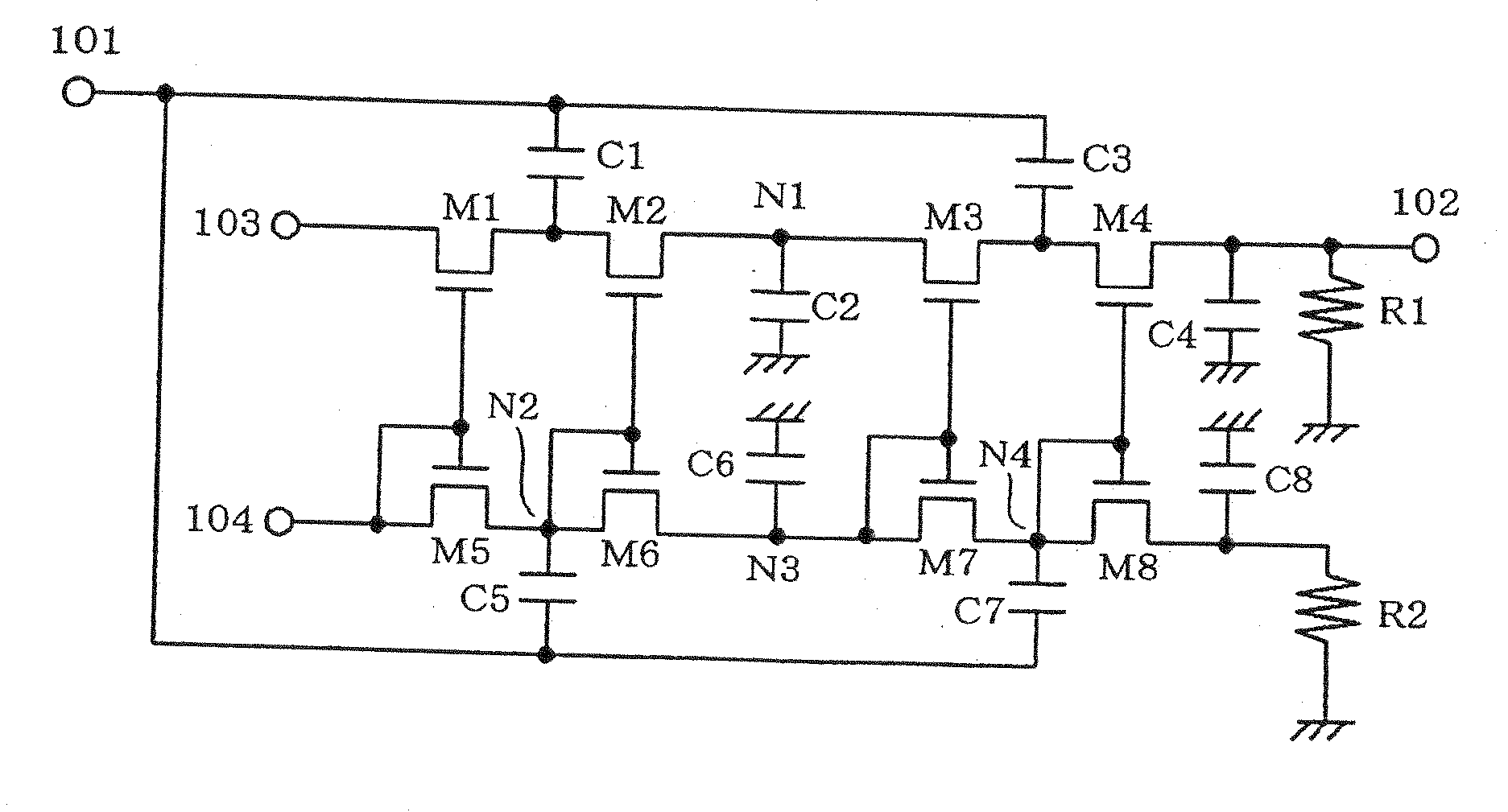
[0031]FIG. 5 is a circuit diagram showing a start signal detector circuit according to a first exemplary embodiment of the present invention. The start signal detector circuit according to this exemplary embodiment includes a rectifier circuit including two stages of half-wave voltage doubler rectifier circuits cascaded to each other shown in the upper part of the drawing and a bias circuit having the same configuration as the rectifier circuit shown in the lower part of the drawing. In FIG. 5, 101 denotes an RF input terminal, 102 denotes an output terminal, 103, 104 denote DC bias terminals, M1 to M8 denote MOS transistors, C1 to C8 denote capacitors, and R1, R2 denote resistors. In this circuit, a constant DC voltage is applied to DC bias terminal 103, and a voltage equal to the sum of the voltage applied to DC bias terminal 103 and the amount of a variation ΔVt of the threshold voltage of the MOS transistors is applied to DC bias terminal 104. In the negative half cycle of a sig...
exemplary embodiment 2
[0035]FIG. 6 is a circuit diagram showing a start signal detector circuit according to a second exemplary embodiment of the present invention. The start signal detector circuit according to this exemplary embodiment is the start signal detector circuit according to the first exemplary embodiment additionally provided with a circuit that produces a DC bias. In FIG. 6, 101 denotes an RF input terminal, 102 denotes an output terminal, 105 denotes a power supply terminal, M1 to M9 denote MOS transistors, C1 to C8 denote capacitors, and R1 to R5 denote resistors. The start signal detector circuit according to the second exemplary embodiment shown in FIG. 6 includes a two-stage half-wave voltage doubler rectifier circuit including MOS transistors M1 to M4 and capacitors C1 to C4, a bias circuit, which is a two-stage half-wave voltage doubler rectifier circuit including MOS transistors M5 to M8 and capacitors C5 to C8, and a circuit for detecting a threshold variation and for producing a D...
exemplary embodiment 3
[0039]FIG. 7 is a circuit diagram showing a start signal detector circuit according to a third exemplary embodiment of the present invention. The start signal detector circuit according to this exemplary embodiment is the start signal detector circuit according to the first exemplary embodiment additionally provided with a circuit that produces a DC bias. In FIG. 7, 101 denotes an RF input terminal, 102 denotes an output terminal, 105 denotes a power supply terminal, M1 to M9 denote MOS transistors, C1 to C8 denote capacitors, and R1, R2, R6 to R9 denote resistors. In the start signal detector circuit according to the third exemplary embodiment shown in FIG. 7, a two-stage half-wave voltage doubler rectifier circuit including MOS transistors M1 to M4 and capacitors C1 to C4 and a bias circuit, which is a two-stage half-wave voltage doubler rectifier circuit including MOS transistors M5 to M8 and capacitors C5 to C8, conduct the same operation as the circuits according to the first e...
PUM
 Abstract
Description
Claims
Application Information
 - R&D
- Intellectual Property
- Life Sciences
- Materials
- Tech Scout
- Unparalleled Data Quality
- Higher Quality Content
- 60% Fewer Hallucinations
Browse by: Latest US Patents, China's latest patents, Technical Efficacy Thesaurus, Application Domain, Technology Topic, Popular Technical Reports.
© 2025 PatSnap. All rights reserved.Legal|Privacy policy|Modern Slavery Act Transparency Statement|Sitemap|About US| Contact US: help@patsnap.com