

Method for Manufacturing Light-Emitting Device
a technology of light-emitting devices and manufacturing methods, which is applied in the manufacture of electric discharge tubes/lamps, cold cathode manufacturing, and the manufacture of electromechanical systems, etc., can solve the problems of difficult to maintain a constant evaporation rate, difficult to precisely control the evaporation rate of each host material and dopant material, and difficult to form a layer. , to achieve the effect of accurate and easy-to-form layer
- Summary
- Abstract
- Description
- Claims
- Application Information
AI Technical Summary
Benefits of technology
Problems solved by technology
Method used
Image

Examples
embodiment mode 1
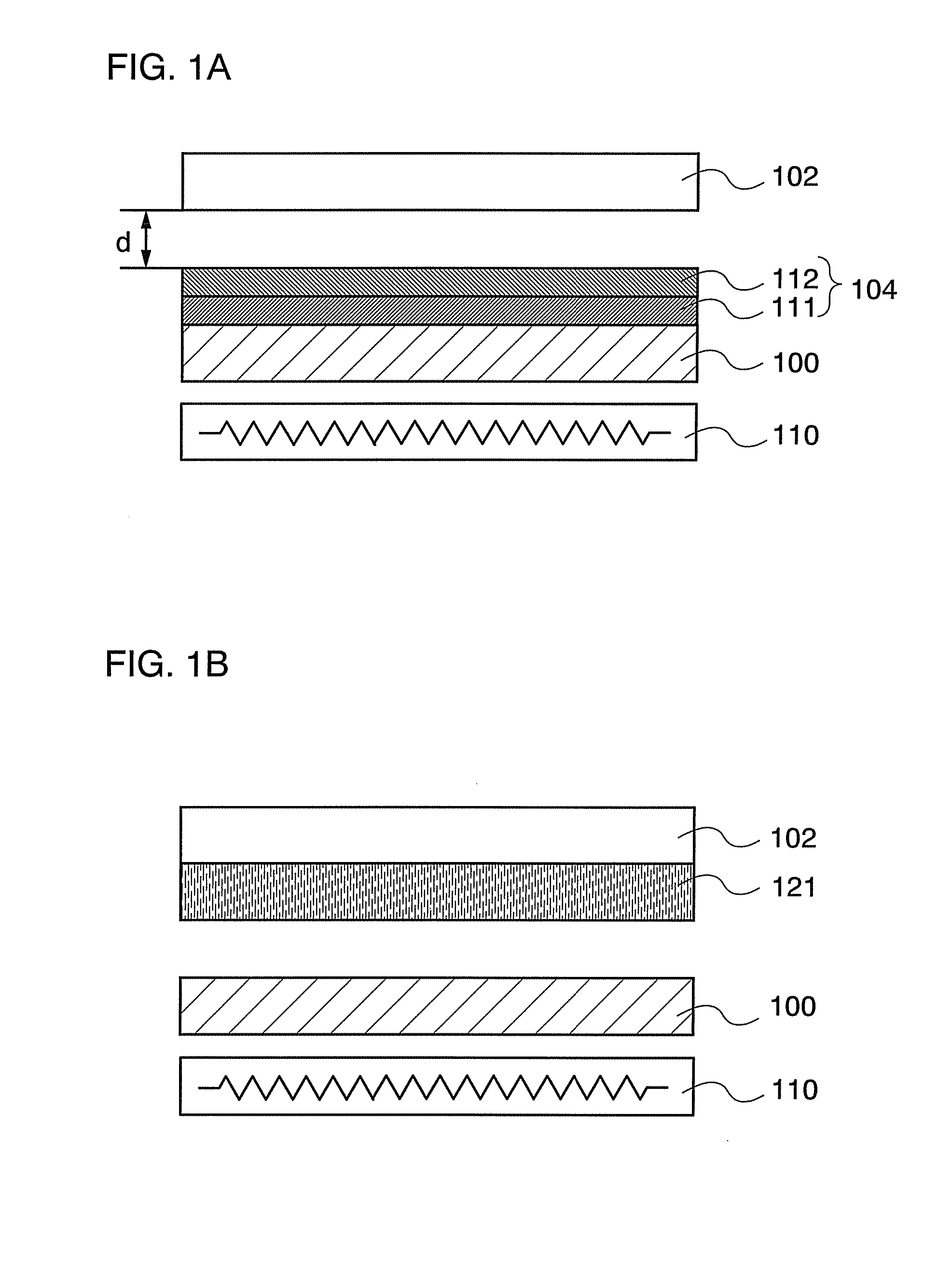
[0043]A method for manufatcuring a light-emitting device of the present invention will be described with reference to FIGS. 1A and 1B.
[0044]In FIGS. 1A and 1B, a plurality of layers 104 containing evaporation materials is stacked over a first substrate 100. These layers serve as an evaporation source of the present invention. In the evaporation source of the present invention, the plurality of layers containing evaporation materials is stacked, and thus, contrary to a co-evaporation method, the evaporation source is a single unit even though it contains a plurality of evaporation materials.
[0045]The first substrate 100 is a substrate for forming the plurality of layers containing evaporation materials which serves as an evaporation source. The substrate 100 serves as a supporting substrate of the plurality of layers containing evaporation materials. As the first substrate 100, for example, the following can be used: an oxide substrate made of quartz, ceramic, sapphire, or the like, ...
embodiment mode 2
[0074]In this embodiment mode, a manufacturing method of a light-emitting device, to which the present invention is applied, will be described.
[0075]For example, light-emitting elements shown in FIGS. 3A and 3B can be manufactured. In the light-emitting element shown in FIG. 3A, a first electrode layer 302, an EL layer 308 which functions as a light-emitting layer 304, and a second electrode layer 306 are stacked in this order over a substrate 300. One of the first electrode layer 302 and the second electrode layer 306 functions as an anode, and the other functions as a cathode. Holes injected from the anode and electrons injected from the cathode are recombined in the light-emitting layer 304, whereby light emission can be obtained. In this embodiment mode, the light-emitting layer 304 is formed of a mixed layer in which a very small amount of dopant material which is a light-emitting material is dispersed in a host material. In addition, the first electrode layer 302 functions as ...
embodiment mode 3
[0135]In this embodiment mode, an example of a deposition apparatus which makes it possible to manufacture a light-emitting device of the present invention will be described. FIGS. 9A to 9C and FIGS. 10A to 10C are each a schematic view of a cross section of a deposition apparatus of this embodiment mode.
[0136]In FIG. 9A, a deposition chamber 801 is a vacuum chamber, which is connected to other treatment chambers via a first gate valve 802 and a second gate valve 803. In addition, the deposition chamber 801 is provided with at least a substrate supporting unit which is a first substrate supporting unit 804, a deposition substrate supporting unit which is a second substrate supporting unit 805, and a heater which is capable of vertical movement as a heat source 806.
[0137]First, in another deposition chamber, a material layer 808 is formed over a first substrate 807 which is a supporting substrate. In this embodiment mode, the first substrate 807 corresponds to the first substrate 100...
PUM
| Property | Measurement | Unit |
|---|---|---|
| Temperature | aaaaa | aaaaa |
| Evaporation enthalpy | aaaaa | aaaaa |
Abstract
Description
Claims
Application Information