Optical device and method of controlling the same

a technology of optical semiconductor elements and control methods, applied in the field of optical devices, to achieve the effect of stabilizing the heat value of the heater and restricting the temperature change of the optical semiconductor elements

Active Publication Date: 2009-01-22
SUMITOMO ELECTRIC DEVICE INNOVATIONS
View PDF2 Cites 12 Cited by
  • Summary
  • Abstract
  • Description
  • Claims
  • Application Information

AI Technical Summary

Benefits of technology

[0017]With the method, the temperature changing of the optical semiconductor element is restrained with use of the temperature control device. Further, the heat value of the heater may be stabilized, because the electrical power provided to the heater is controlled to be kept constant. In this case, desired optical property may be obtained even if the heater is degraded.

Problems solved by technology

That is, the temperature of the optical waveguide is substantially determined by the heat value of the heater, because the temperature changing of the optical device caused by outer environmental changing may be neglect.

Method used


Image

  • Optical device and method of controlling the same
  • Optical device and method of controlling the same
  • Optical device and method of controlling the same

Examples


first embodiment

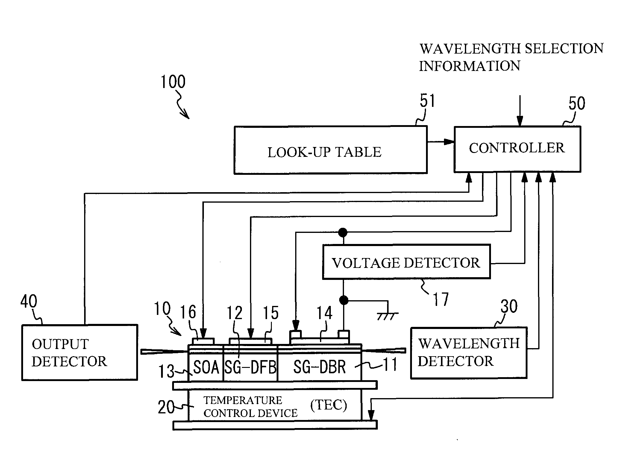
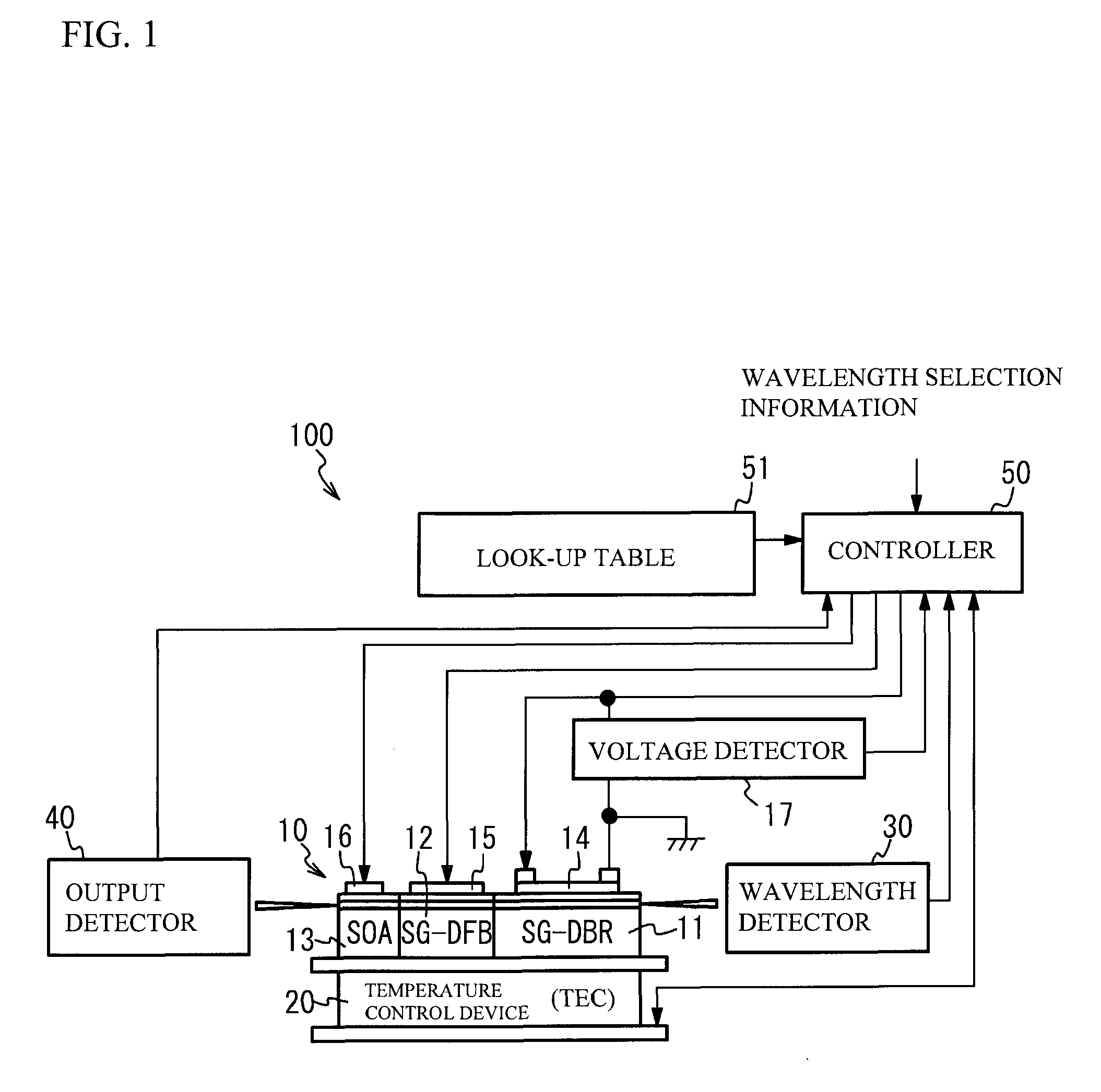
[0027]A description will be given of a semiconductor laser as an optical element. FIG. 1 illustrates a semiconductor laser 10 in accordance with a first embodiment and a structure of a laser device 100 having the semiconductor laser 10. As shown in FIG. 1, the laser device 100 has the semiconductor laser 10, a temperature control device 20, a wavelength detector 30, an output detector 40 and a controller 50. The semiconductor laser 10 is mounted on the temperature control device 20. A description will be given of each part.

[0028]The semiconductor laser 10 has a structure in which a SG-DBR region 11, a SG-DFB region 12 and a semiconductor amplifier (SOA: Semiconductor Optical Amplifier) region 13 are coupled in order. The SG-DBR region 11 has an optical waveguide in which gratings are provided at a given interval. That is, the optical waveguide of the SG-DBR region 11 has a first region that has a diffractive grating and a second region that is optically connected to the first region...

second embodiment

[0050]In a second embodiment, a description will be given of a semiconductor laser having the above-mentioned CSG-DBR. FIG. 5 illustrates a semiconductor laser 10a and a structure of a laser device 100a having the semiconductor laser 10a. As shown in FIG. 5, the semiconductor laser 10a has a CSG-DBR region 11a instead of the SG-DBR region 11. In the embodiment, the CSG-DBR region 11a has three segments having a combination of a grating and a spacer region. Accordingly, three heaters 14a, 14b and 14c are provided on the CSG-DBR region 11a according to each of the segments. And voltage detectors 17a, 17b and 17c are provided according to each of the heaters.

[0051]In the embodiment, it is possible to keep the heat value of each heater constant when the electrical power provided to each of the heaters is feedback controlled to be kept constant according to the detection result of each of the voltage detector. Therefore, the semiconductor laser 10a obtains a desired oscillation wavelengt...

third embodiment

[0053]The present invention may be applied to an optical element other than a semiconductor laser. For example, the present invention may be applied to a mach-Zehnder optical switch. This optical switch is used in an exchange system such as an optical cross connect.

[0054]FIG. 6 illustrates a structure of an optical switch 200 in accordance with a third embodiment. As shown in FIG. 6, the optical switch 200 is made of a material having a thermooptical effect such as silica-based material. The optical switch 200 has a mach-Zehnder interference structure having a first waveguide 201 and a second waveguide 202. The optical switch 200 is arranged on a temperature control device 210. Therefore, the temperature control device 210 controls temperature of each part thereof.

[0055]The optical switch 200 has a heater 203. The heater 203 heats the second waveguide 202. This results in a changing of a phase differential between a light transmitting in the first waveguide 201 and a light transmitt...


PUM


Abstract

An optical device includes an optical element, a detector and a controller. The optical element has an optical waveguide. Refractive index of the optical waveguide is controlled by a heater. A temperature of the optical element is controlled by a temperature control device. The detector detects a current flowing in the heater and / or a voltage applied to the heater. The controller controls an electrical power provided to the heater so as to be kept constant according to the detection result of the detector.

Description

BACKGROUND OF THE INVENTION[0001]1. Field of the Invention[0002]The present invention relates an optical device and a method of controlling the optical device.[0003]2. Description of the Related Art[0004]A wavelength tunable semiconductor laser is one of optical devices. The wavelength tunable semiconductor laser has a gain for a laser oscillation and selects wavelength.[0005]There is a method of tuning wavelength characteristics of loss, reflection or gain by tuning refractive index of an optical functional region such as a diffractive grating provided in an optical waveguide in a resonator, as a method of selecting wavelength.[0006]The method of tuning the refractive index does not need a mechanical movable portion, being different from a method of tuning a mechanical angle or a mechanical length. Therefore, the method has an advantage in reliability and a manufacturing cost. There is a method of tuning a temperature of an optical waveguide, a method of tuning a carrier density in...

Claims


Application Information

Patent Timeline
Patent Type & Authority Applications(United States)
IPC IPC(8): G01R1/44G01R23/04H01S3/04
CPCG02F1/0121G02F1/0147G02F1/3136G02F2201/307G02F2201/346H01S5/024H01S5/125H01S5/0261H01S5/0612H01S5/0617H01S5/0687H01S5/1209H01S5/02415
Inventor ISHIKAWA, TSUTOMUMACHIDA, TOYOTOSHITANAKA, HIROKAZU
Owner SUMITOMO ELECTRIC DEVICE INNOVATIONS
Why Eureka
Try Eureka