Semiconductor Light Emitting Element

a technology of light-emitting elements and semiconductors, which is applied in the direction of basic electric elements, semiconductor devices, electrical equipment, etc., can solve the problems of difficult to cause the recombination of electrons and holes, difficulty in achieving light-emitting power, and inability to achieve high brightness, etc., to achieve the effect of increasing the light-emitting ratio, increasing the light-emitting amount and high brightness

Inactive Publication Date: 2009-01-29
ROHM CO LTD
View PDF6 Cites 30 Cited by
  • Summary
  • Abstract
  • Description
  • Claims
  • Application Information

AI Technical Summary

Benefits of technology

[0008]The present invention has been proposed under the circumstances described above. It is, therefore, an object of the present invention is to provide a semi...

Problems solved by technology

Thus, it is difficult to cause the recombination of electrons and holes to occur at the entire region of the active layer 93.
As a result, in t...

Method used


Image

  • Semiconductor Light Emitting Element
  • Semiconductor Light Emitting Element
  • Semiconductor Light Emitting Element

Examples


first embodiment

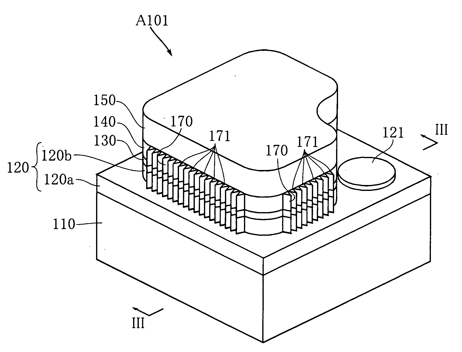
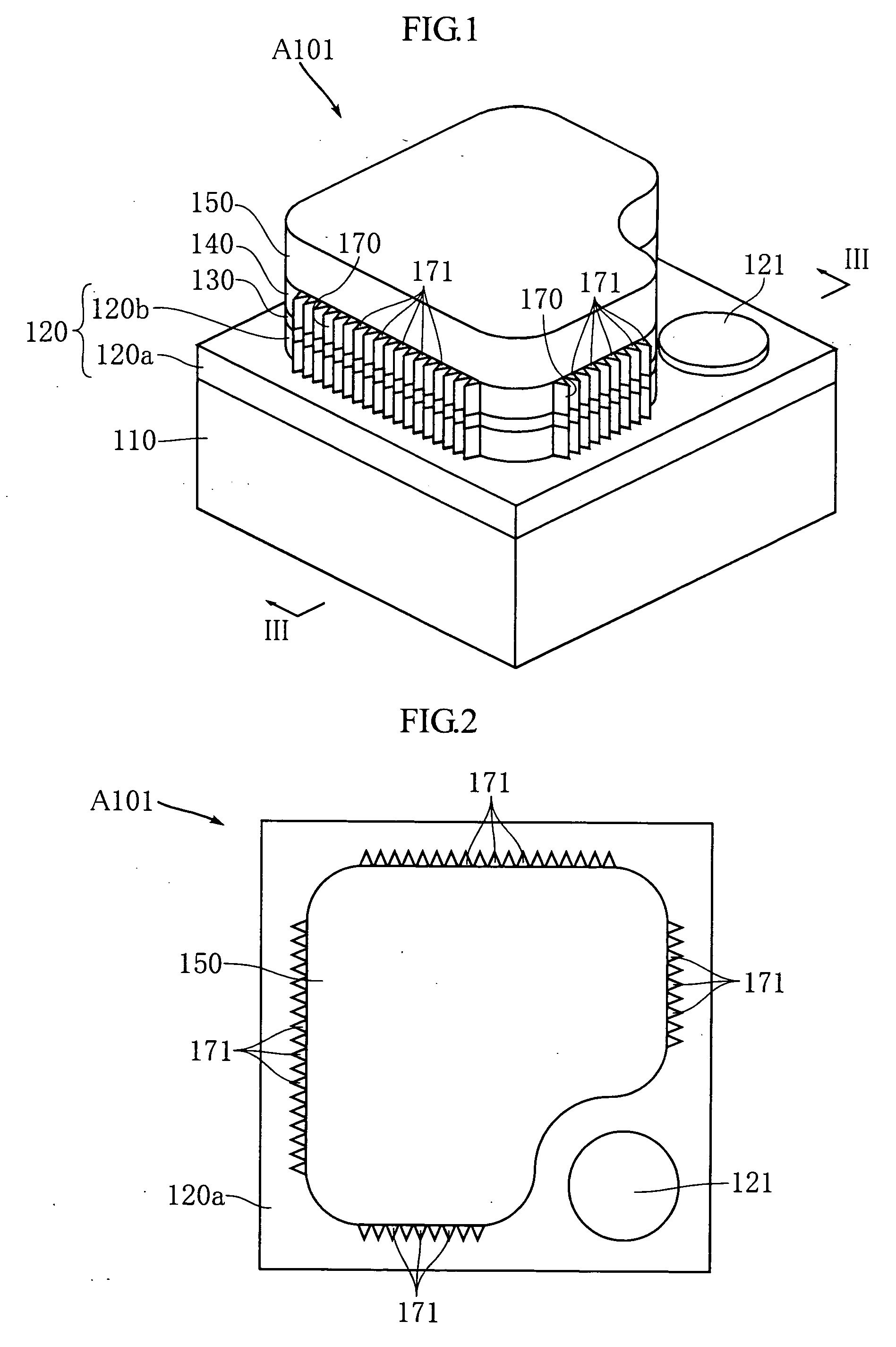
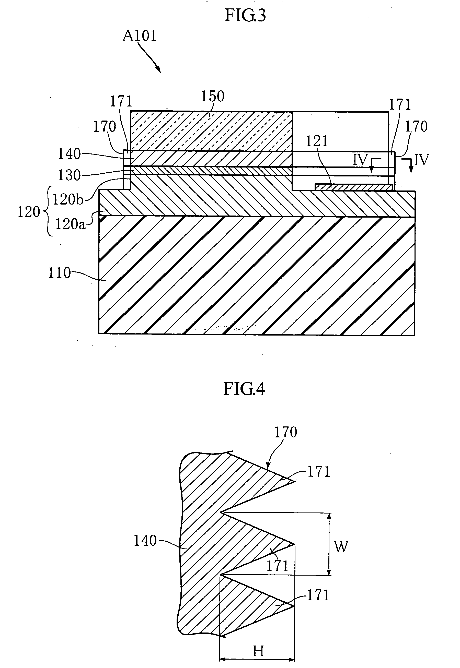
[0066]FIGS. 1-3 show a semiconductor light emitting element according to the present invention. The semiconductor light emitting element A101 of this embodiment includes a substrate 110, an n-GaN layer 120, an active layer 130, a p-GaN layer 140 and a ZnO electrode 150. The semiconductor light emitting element A101 is particularly designed to emit blue light or green light.

[0067]The substrate 110 is made of e.g. sapphire and supports the n-GaN layer 120, the active layer 130, the p-GaN layer 140 and the ZnO electrode 150. In this embodiment, the substrate 110 has a thickness of about 80 μm. A buffer layer (not shown) made of e.g. AlN, GaN or AlGaN to alleviate lattice strain is formed on the substrate 110.

[0068]The n-GaN layer 120 is made of an n-type semiconductor formed by doping Si into GaN and an example of n-type semiconductor layer of the present invention. In this embodiment, the n-GaN layer 120 has a thickness of about 3 to 6 μm. As shown in FIG. 3, the n-GaN layer 120 compr...

second embodiment

[0089]FIG. 7 shows a semiconductor light emitting element according to the present invention. The semiconductor light emitting element A102 of this embodiment differs from that of the foregoing embodiment in that a plurality of projections 171 are formed also on the substrate 110 and the first layer 120a of the n-GaN layer 120. The projections 171 of this embodiment have the same cross sectional configuration as that of the projections 171 shown in FIG. 4. The projections 171 can be formed by subjecting the substrate 110 and the n-GaN layer 120 to etching or dicing using a dicing blade formed with triangular grooves.

[0090]According to this embodiment, owing to the provision of the projections 171, the light traveling from the active layer 130 and reaching the first layer 120a of the n-GaN layer 120 and the substrate 110 through the second layer 120b of the n-GaN layer 120 is efficiently emitted. Thus, the semiconductor light emitting element A102 is capable of emitting a larger amou...

third embodiment

[0091]FIGS. 8 and 9 show a semiconductor light emitting element according. to the present invention. The semiconductor light emitting element A103 of this embodiment differs from those of the foregoing embodiments in that a plurality of cone-shaped projections 172 are provided. Further, the lamination structure of the semiconductor light emitting element A103 differs from that of the foregoing embodiments.

[0092]Specifically, the semiconductor light emitting element A103 includes a substrate 110, and an n-GaN layer 120, an active layer 130 and a p-GaN layer 140 which are laminated on one surface side of the substrate 110. The substrate 110 is made of SiC and includes a prismatic portion on the upper side in the figure and a tapered portion on the lower side in the figure. The surface of the substrate 110, which is opposite from the surface formed with the n-GaN layer 120, is formed with an n-side electrode 121. A reflective layer 160 is formed on the lower surface of the p-GaN layer ...


PUM


Abstract

In a semiconductor light emitting element, a p-type layer (220), an active layer (230) and an n-type layer (240) are laminated on a substrate in this order. The n-type layer (240) is formed with a rectangular n-side electrode (241) whose width in one direction is equal to that of the n-type layer (240). The thickness t of the n-type layer (240) satisfies Formula 1 below. The semiconductor light emitting element includes a side surface (270) extending in the lamination direction and formed with a plurality of projections (271). Supposing that the wavelength of the light from the active-layer (230) is λ and the index of refraction of the n-type layer (240) or the p-type layer (220) is n, the average WA of widths at bottoms of the projections is set to satisfy WA≧λ/n.
tρJ0e4γκBT·W(L-W)Formula1
    • where L is width of the n-type layer in a direction different from the one direction,
    • T is absolute temperature,
    • W is width of the n-side electrode in a direction different from the one direction,
    • J0 is current density at the contact portion between the n-side electrode and the n-type layer,
    • e is elementary charge,
    • γ is diode ideality factor,
    • κB is Boltzmann constant,
    • ρ is specific resistance of the n-type semiconductor layer.

Description

TECHNICAL FIELD[0001]The present invention relates to a semiconductor light emitting element including a semiconductor layer.BACKGROUND ART[0002]Conventionally, a semiconductor light emitting element. including a plurality of semiconductor layers containing GaN. and laminated on a sapphire substrate has been proposed (see e.g. Patent Document 1).[0003]In a known method for manufacturing a semiconductor light emitting element, after semiconductor layers are formed on a sapphire substrate, a support substrate is bonded to the semiconductor layers on the side opposite from the sapphire substrate. Then, the sapphire substrate is removed utilizing heat generated by laser beam irradiation (see Patent Document 2, for example). FIG. 20 shows an example of semiconductor light emitting element manufactured by such a method. In the semiconductor light emitting element X shown in the figure, a p-GaN layer 92, an active layer 93 and an n-GaN layer 94 as. semiconductor layers are laminated on a s...

Claims


Application Information

Patent Timeline
IPC IPC(8): H01L33/00H01L33/20H01L33/22H01L33/32
CPCH01L33/20H01L33/32H01L33/22
Inventor SAKAI, MITSUHIKOOKAZAKI, TADAHIRONAKAHARA, KEN
Owner ROHM CO LTD
Why Eureka
Try Eureka