Method for the production of semiconductor granules

Inactive Publication Date: 2009-01-29
STILE
View PDF24 Cites 9 Cited by
  • Summary
  • Abstract
  • Description
  • Claims
  • Application Information

AI Technical Summary

Benefits of technology

[0006]An aspect of the invention includes a method for manufacturing granules adapted to feeding a se

Problems solved by technology

Indeed, if a silicon melt is fed with smaller particles, the particles very uneasily incorporate to the melt, which adversely affects the smooth progress of the process.
To have the grains of these powders grow bigger, specific conditions must be implemented,

Method used


Image

  • Method for the production of semiconductor granules
  • Method for the production of semiconductor granules
  • Method for the production of semiconductor granules

Examples


Example

[0027]To manufacture inexpensive granules, within a short time and while consuming little power, the inventor has thought of sintering or melting semiconductor powders.

[0028]The powders used, for example, are powders of nanometric size (from 10 to 500 nm) or micrometric size (from 10 to 500 μm) coming from the CVD reactors. Silicon wafer sawing residues, which also include powders of nanometric and micrometric size, may also be used.

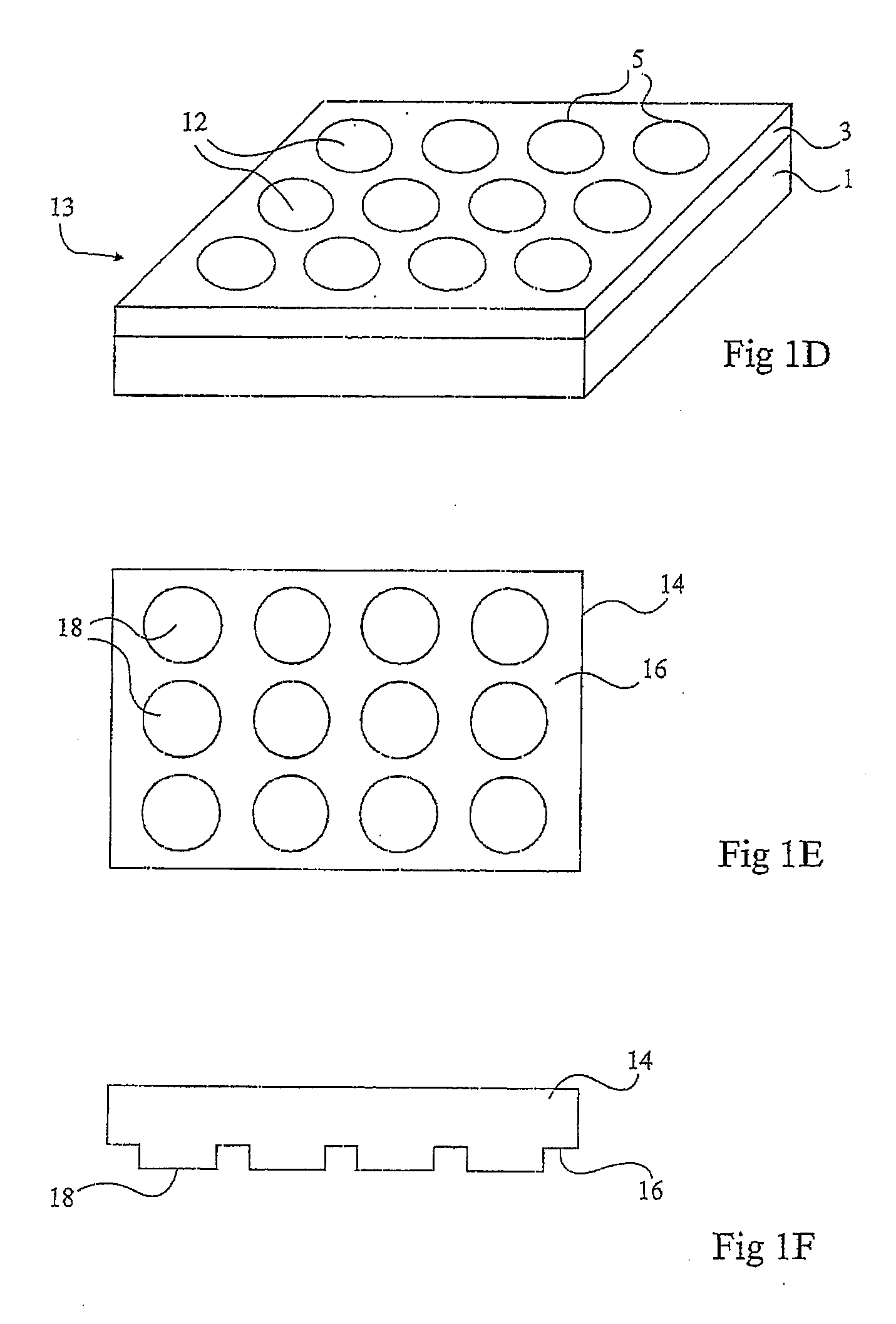
[0029]The granule manufacturing according to an embodiment of the present invention will now be described in relation with FIGS. 1A to 1F.

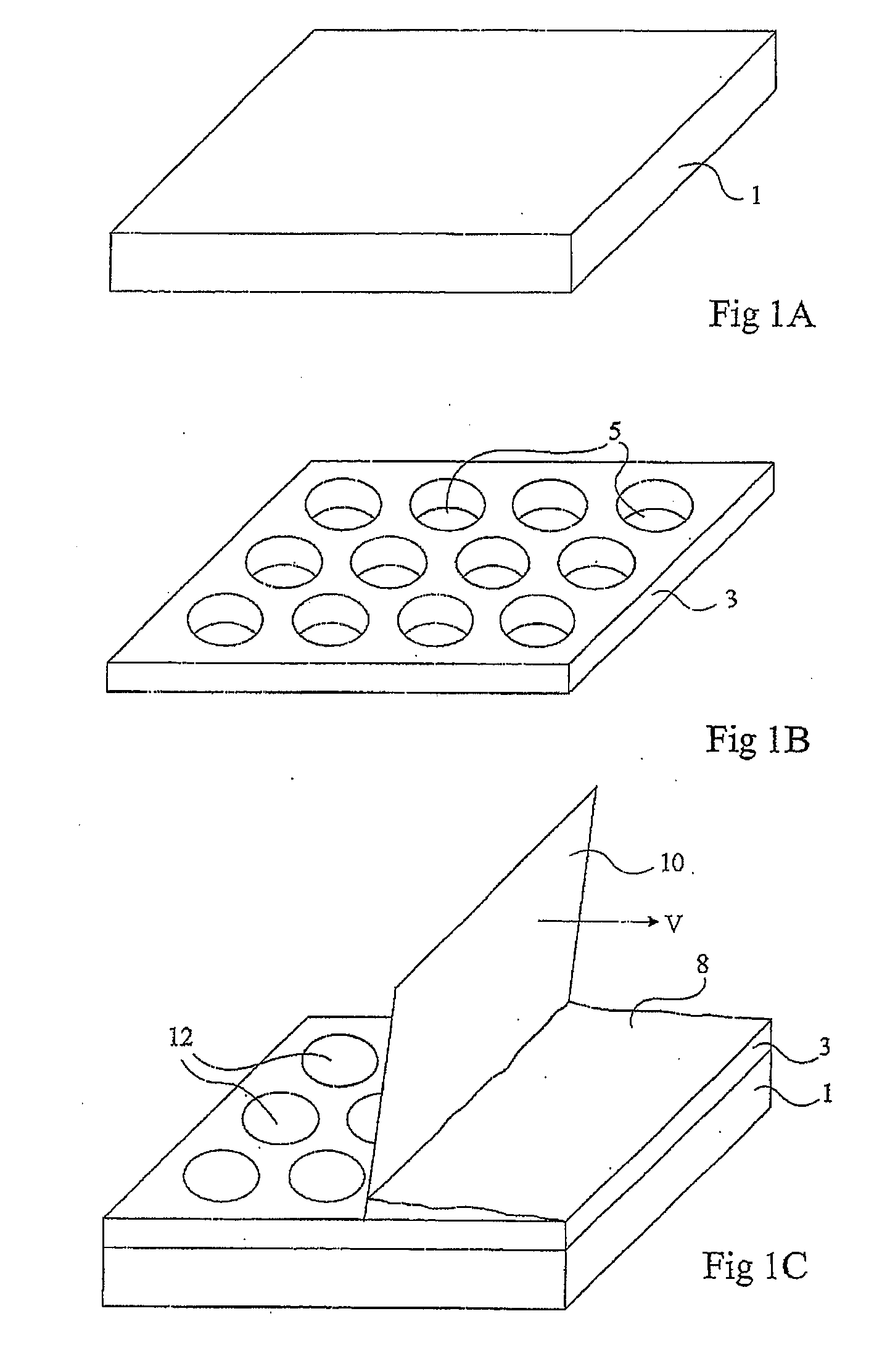
[0030]FIG. 1A shows a planar parallelepipedal-shaped support 1. Support 1 is intended to be a compression part and it is formed, for example, with a graphite blade, or another ceramic. To form support 1, silicon nitride (Si3N4), silicon carbide (SiC), boron nitride (BN), alumina, zirconia, magnesia, etc. may, for example, be used.

[0031]A mould 3, shown in FIG. 1B, is placed above support 1 of FIG. 1A. Mould 3 is a plat...


PUM

PropertyMeasurementUnit
Temperatureaaaaaaaaaa
Lengthaaaaaaaaaa
Lengthaaaaaaaaaa

Abstract

A method of manufacturing a semiconductor material in the form of bricks or granules, includes a step of sintering powders of at least one material selected from the group consisting of silicon, germanium, gallium arsenide, and the alloys thereof so as to form said granules. The sintering step includes the steps of compacting and thermal processing the powders, and a step of purifying the semiconductor material using a flow of a gas. The gas flow passes through the porosity channels of the material.

Description

RELATED APPLICATIONS[0001]This application is a continuation in part of U.S. application Ser. No. 10 / 553,049, filed Oct. 10, 2005 entitled Method For The Production of Semiconductor Granules which is the national stage application under 35 U.S.C. § 371 of the International Application No. PCT / FR2004 / 050152, and claims the benefit of French Application No. 03 / 04675, filed Apr. 14, 2003 and Int'l. Application No. PCT / FR2004 / 050152, filed Apr. 9, 2004, the entire disclosures of which are incorporated herein by reference in their entireties.FIELD OF THE INVENTION[0002]The present invention relates to the field of semiconductor materials, and in particular, but not exclusively, semiconductor granules usable to feed a melt intended for the forming of ingots of a semiconductor material, such as silicon.BACKGROUND OF THE INVENTION[0003]Conventionally, single-crystal silicon or polysilicon ingots are obtained by growth or stretching from silicon melts. Such melts are fed with silicon granule...

Claims


Application Information

Patent Timeline
IPC IPC(8): B22F5/10B08B3/08B08B5/00
CPCB01J2/22B22F3/12B22F2998/10B22F2999/00C30B11/00C30B15/00C30B29/06B22F3/02B22F3/15B22F3/24B22F2201/013B22F2201/00
Inventor STRABONI, ALAIN
Owner STILE
Why Eureka
Try Eureka