Image displaying device

Inactive Publication Date: 2009-02-05
PANASONIC LIQUID CRYSTAL DISPLAY CO LTD +1
View PDF6 Cites 19 Cited by
  • Summary
  • Abstract
  • Description
  • Claims
  • Application Information

AI Technical Summary

Benefits of technology

[0028]The image displaying device having any one of the configurations described above can thus suppress the leak

Problems solved by technology

Consequently, a high electric field is induced mainly to a depletion layer formed in the semiconductor layer, thereby a leak current is generated and the dark current increases easily.
This has prevented the improvement of th

Method used


Image

  • Image displaying device
  • Image displaying device
  • Image displaying device

Examples


Example

First Embodiment

(Configuration)

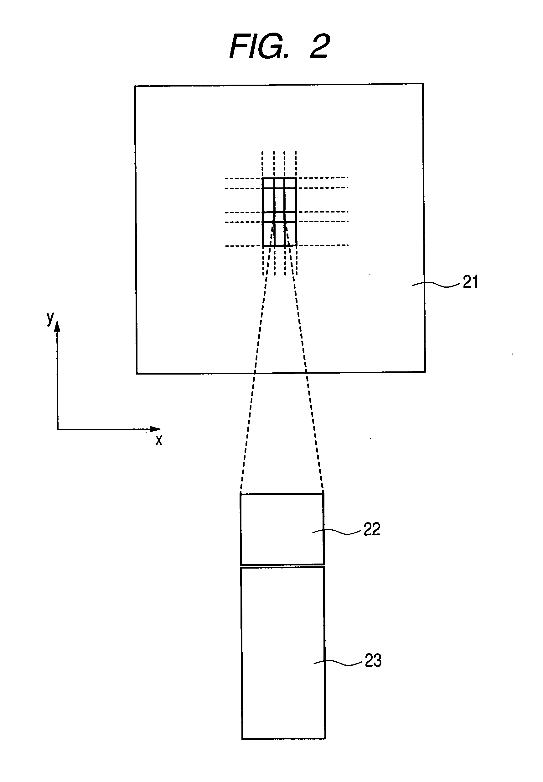
[0055]FIG. 2 shows a top view of an image display area 21 of an image displaying device (e.g., liquid crystal display device) of the present invention. In this area 21 are disposed many pixels 23 in a matrix pattern and a photosensing device 22 is disposed between each pair of adjacent pixels 23 positioned, for example, in the y direction in FIG. 2.

[0056]In other words, similarly to the pixels 23, the photosensing devices 22 are disposed in a matrix pattern. Each photosensing device 22 is shifted in the y direction from its corresponding pixel 23 and disposed between pixels 23 that are adjacent to each other in the y direction.

[0057]In this first embodiment, at a top view, the area of each photosensing device 22 is smaller than that of each pixel 23. This is because each pixel 23 is required to have an aperture ratio preferentially.

[0058]Consequently, because each pixel 23 in the image displaying area 21 can be driven independently to visualize an imag...

Example

Second Embodiment

(Configuration)

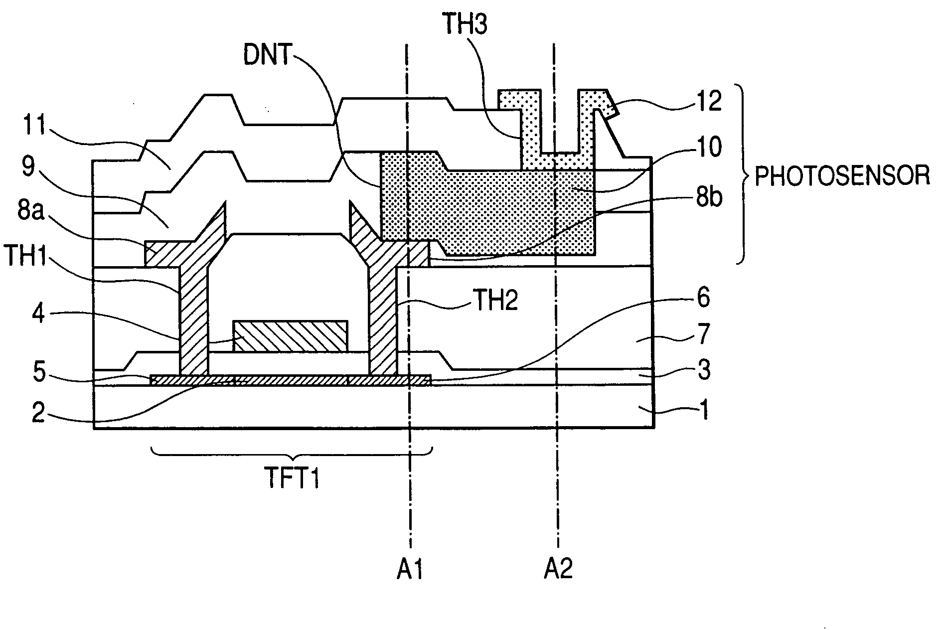
[0121]FIG. 6 is a cross sectional view of a major portion of a liquid crystal display device of the present invention, which corresponds to FIG. 1.

[0122]The configuration of the liquid crystal display device of the present invention in this second embodiment differs from that shown in FIG. 1 as follows. The first drain electrode 138b and the second drain electrode 140 of the thin film transistor TFT1 are connected to the semiconductor layer 10 of the photo sensor LS through the transparent electrode wiring 143 consisting of a transparent conductive layer and the electrode wiring 8c connected to the semiconductor layer 10 is formed in the same layer as the drain electrode 138b.

[0123]In other words, the electrode wiring 8c is formed in the same layer as the drain electrode 138b on the surface of the first interlayer dielectric film 7.

[0124]And the second drain electrode 140 is formed on the second interlayer dielectric film 9 in which the semiconductor...

Example

Third Embodiment

(Configuration)

[0144]FIG. 7 shows a configuration of an image displaying device of the present invention in a third embodiment. The configuration in this FIG. 7 corresponds to that in FIG. 3.

[0145]The configuration in this FIG. 7 differs significantly from that in FIG. 3. The differences are the thin film transistor TFT 1 of the photo sensor 22 and the thin film transistor TFT 2 of the pixel 23. The gate electrode wirings 4 and 31 of the thin film transistor TFT 1 and 2 are disposed under the semiconductor layers 44a and 54 respectively (referred to as so-called bottom gate type ones).

[0146]This is why the connection between the thin film transistor TFT 1 and the photo sensor LS comes to be slightly different from that in the configurations described in the above embodiments.

[0147]FIG. 8 shows a cross sectional view taken on line VIII-VIII of FIG. 7A.

[0148]In FIG. 8, a gate electrode wiring 4 is formed on the surface of the substrate 1 at the side closer to the liqui...


PUM


Abstract

An image displaying device having multiple photosensing devices have successfully suppressed a leakage current from each photosensing device and improved the S/N ratio. In the image displaying device, pixels and photosensing devices are disposed as pairs in a matrix pattern on a substrate. Each of the pixels and each of the photosensing devices are driven independently. Each photosensing device includes a semiconductor layer that is a photoelectric conversion layer connected to at least a first electrode and a second electrode. The contact surfaces of the first and second electrodes with respect to the semiconductor layer are disposed so that their center axes are separated from each other.

Description

CLAIM OF PRIORITY[0001]The present application claims priority from Japanese patent application JP 2007-196996 filed on Jul. 30, 2007, the content of which is hereby incorporated by reference into this application.FIELD OF THE INVENTION[0002]The present invention relates to an image displaying device, more particularly to an image displaying device having a plurality of built-in photosensing devices.BACKGROUND OF THE INVENTION[0003]There is a well-known liquid crystal display device used, for example, for mobile phones or on-vehicle units / devices. The display device includes a touch panel function mechanism allowing input operations from the touch panel.[0004]Among such touch panel function mechanisms, there is a well-known one formed by integrating its sensors and pixels at one-to-one correspondence in the liquid crystal display device.[0005]Each sensor is configured by a photo sensor with Schottky-barrier configured so as to have a metal layer and a semiconductor layer with a junc...

Claims


Application Information

Patent Timeline
IPC IPC(8): H01L33/00G02F1/1333G02F1/1368G09F9/00G09F9/30H01L27/146H01L31/10
CPCG09G3/20H01L27/1214H01L27/14643H01L27/14692
Inventor SUZUMURA, ISAOTOYOTA, YOSHIAKI
Owner PANASONIC LIQUID CRYSTAL DISPLAY CO LTD
Why Eureka
Try Eureka