Multi-chip stack structure having through silicon via and method for fabrication the same

a stack structure and silicon via technology, applied in the direction of semiconductor devices, semiconductor/solid-state device details, electrical apparatus, etc., can solve the problems of increasing the use area of the substrate and the fabrication cost, affecting the quality of the electrical connection between the chips and the substrate, and the number of chips that can be received by the package is also limited, so as to avoid contamination, save fabrication cost, and simplify the fabrication process

Inactive Publication Date: 2009-02-05
SILICONWARE PRECISION IND CO LTD
View PDF6 Cites 89 Cited by
  • Summary
  • Abstract
  • Description
  • Claims
  • Application Information

AI Technical Summary

Benefits of technology

[0020]Therefore, the present invention mainly comprises forming a plurality of holes on the first surface of the wafer having a plurality of first chips and forming metal posts and solder pads corresponding to the holes so as to form a TSV structure; forming at least one groove on the second surface of each of the first chips to expose the metal posts of the TSV structure such that at least a second chip can be stacked on the first chip and received in the groove and electrically connected to the metal posts exposed from the groove, thereby forming a vertical stack structure of the first chip and the second chip; subsequently filling a insulating material in the grooves to encapsulate the second chips and flattening the insulating material so as to mak

Problems solved by technology

Accordingly, a large die attachment area is required on the substrate for attachment of a large number of chips, thus increasing the use area of the substrate and the fabrication cost.
However, since the chips of the stack structure are electrically connected to the substrate through wire bonding, quality of electrical connections between the chips and the substrate are adversely affected by length of the bonding wires.
Meanwhile, sin

Method used


Image

  • Multi-chip stack structure having through silicon via and method for fabrication the same
  • Multi-chip stack structure having through silicon via and method for fabrication the same
  • Multi-chip stack structure having through silicon via and method for fabrication the same

Examples


first embodiment

[0027]FIGS. 2A to 2F are diagrams showing a multi-chip stack structure having through silicon via (TSV) and a method for fabricating the same according to a first embodiment of the present invention.

[0028]As shown in FIG. 2A, a wafer 21a comprising a plurality of first chips 21 is provided. The wafer 21a and the first chips 21 each have a first surface 211 and a second surface 212 opposed to the first surface 211. A plurality of holes 210 is formed on the first surface 211 of each of the first chips 21, and metal posts 23 and solder pads 231 are formed corresponding to the holes 210 so as to form a TSV structure.

[0029]An insulating layer 23″ made of such as silicon dioxide or silicon nitride is disposed between the holes 210 and the metal posts 23, and a barrier layer 23′ made of such as nickel is disposed between the insulating layer 23″ and the metal posts 23. The metal posts 23 are made of such as copper, gold or aluminum.

[0030]As shown in FIG. 2B, at least a groove 2120 is forme...

second embodiment

[0038]FIGS. 3A to 3D are diagrams showing a multi-chip stack structure having TSV and a method for fabricating the same according to a second embodiment of the present invention. The elements of the present embodiment that are same as or similar to those of the above-described embodiment are denoted by the same reference numerals.

[0039]The present embodiment is mostly similar to the first embodiment, a main difference therebetween is TSV is formed in the second chip such that a third chip can be vertically stacked on the second chip and electrically connected to the second chip, thereby enhancing electrical performance of the whole structure.

[0040]As shown in FIG. 3A, at least a second chip 22 is disposed in the groove 2120 of the second surface 212 of the first chip 21 and electrically connected to the metal posts 23 of the first chip 21 exposed from the groove 2120, wherein the second chip 22 has metal posts 223 formed therein so as to form a TSV structure. An insulating material ...

third embodiment

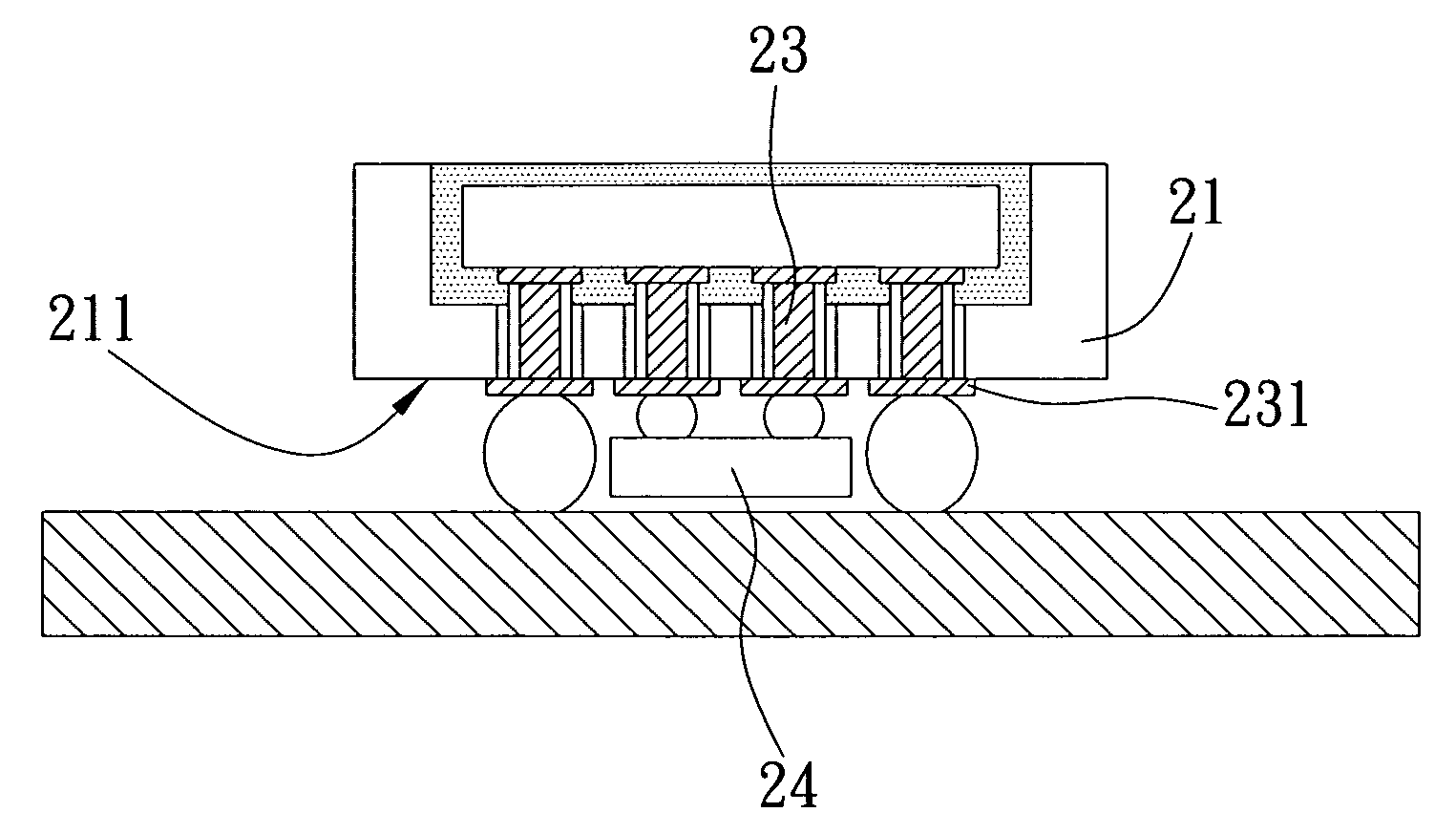
[0045]FIG. 4 is a diagram showing a multi-chip stack structure having TSV and a method for fabricating the same according to a third embodiment of the present invention. For simplification, the elements same as or similar to the above-described embodiments are denoted by the same reference numerals.

[0046]The present embodiment is mostly similar to the above-described embodiments, a main difference of the present embodiment from the above-described embodiments is at least a fourth chip 24 is further disposed on the first surface 211 of the first chip and electrically connected to the solder pads 231 on the first surface 211 of the first chip 12, thereby enhancing electrical performance of the whole structure.


PUM


Abstract

The invention discloses a multi-chip stack structure having through silicon via and a method for fabricating the same. The method includes: providing a wafer having a plurality of first chips; forming a plurality of holes on a first surface of each of the first chips and forming metal posts and solder pads corresponding to the holes so as to form a through silicon via (TSV) structure; forming at least one groove on a second surface of each of the first chips to expose the metal posts of the TSV structure so as to allow at least one second chip to be stacked on the first chip, received in the groove and electrically connected to the metal posts exposed from the groove; filling the groove with an insulating material for encapsulating the second chip; mounting conductive elements on the solder pads of the first surface of each of the first chips and singulating the wafer; and mounting and electrically connecting the stacked first and second chips to a chip carrier via the conductive elements. The wafer, which is not totally thinned but includes a plurality of first chips, severs a carrying purpose during the fabrication process and thereby solves problems, namely a complicated process, high cost, and adhesive layer contamination, facing the prior art that entails repeated use of a carrier board and an adhesive layer for vertically stacking a plurality of chips and mounting the stacked chips on a chip carrier.

Description

BACKGROUND OF THE INVENTION[0001]1. Field of the Invention[0002]The present invention relates generally to semiconductor devices and method for fabricating the same, and more particularly to a multi-chip stack structure having through silicon via (TSV) and a method for fabricating the same.[0003]2. Description of Related Art[0004]A conventional multi-chip module (MCM) semiconductor package comprises two or more chips, which are disposed to a common substrate, horizontally spaced from each other, and electrically connected to the substrate by wire bonding. However, to prevent miscontact between conductive wires of the chips, a certain interval is required between the chips. Accordingly, a large die attachment area is required on the substrate for attachment of a large number of chips, thus increasing the use area of the substrate and the fabrication cost.[0005]U.S. Pat. No. 6,538,331 discloses a chip stack structure with a first chip and a second chip stack disposed on a substrate, w...

Claims


Application Information

Patent Timeline
IPC IPC(8): H01L23/52H01L21/00
CPCH01L23/481H01L25/0657H01L2224/97H01L2224/94H01L2224/73204H01L2224/32145H01L2224/16225H01L2224/16145H01L2224/14181H01L25/50H01L29/0657H01L2224/16H01L2225/06513H01L2225/06541H01L2225/06555H01L2924/01079H01L24/94H01L24/97H01L2224/81H01L2924/00012H01L24/03H01L24/13H01L24/16H01L2224/05001H01L2224/05023H01L2224/05124H01L2224/05144H01L2224/05147H01L2224/05155H01L2224/05568H01L2224/0557H01L2224/13009H01L2224/16146H01L2924/00014H01L2924/10158H01L2224/05599
Inventor CHIANG, CHIANG-CHENGHUANG, CHIEN-PINGCHANG, CHIN-HUANGCHIU, CHI-HSINHUANG, JUNG-PIN
Owner SILICONWARE PRECISION IND CO LTD
Why Eureka
Try Eureka