Exposure method and electronic device manufacturing method

a technology of electronic devices and manufacturing methods, applied in the direction of photomechanical equipment, instruments, and semiconductor/solid-state device details, etc., can solve the problems of difficult to maintain sufficient high productivity, reduce the throughput (processing capacity) of exposure equipment, and take a long time for the detection of every mark position, etc., to achieve rapid and accurate measurement of deformation, improve the accuracy of superimposing patterns on the substrate, and improve the effect of accuracy

Inactive Publication Date: 2009-02-12
NIKON CORP
View PDF33 Cites 18 Cited by
  • Summary
  • Abstract
  • Description
  • Claims
  • Application Information

AI Technical Summary

Benefits of technology

[0012]It is an object of the embodiment according to the present invention to provide an exposure method enabling rapid and accurate measurement of deformation occurring in a unit exposure field and enabling the superimposition of patterns on a substrate with high accuracy.
[0017]In the embodiment according to the present invention, the accuracy for superimposing patterns on the substrate is improved by modifying the shape of a bright-dark pattern exposed on the substrate in correspondence with deformation of an existing pattern formed in the unit exposure field. In this manner, the exposure method of the embodiment according to the present invention enables rapid and accurate measurement of deformation occurring in the unit exposure field based on a plurality of position detection marks that are formed in a predetermined distribution. Thus, patterns are superimposed on the substrate with high accuracy. As a result, the exposure method of the embodiment according to the present invention enables an electronic device to be manufactured with high accuracy.

Problems solved by technology

A conventional position detection apparatus, which includes the single position detection mechanism or the two position detection mechanisms, sequentially detects the positions of the marks and thus takes much time for the detection of every mark position.
This lowers the throughput (processing capacity) of the exposure apparatus and makes it difficult to maintain sufficiently high productivity.
In this case, the distribution of the position detection marks is too rough.
Thus, it is difficult to measure deformation occurring in the unit exposure field, especially, deformation occurring in the LSI circuit patterns with high accuracy.

Method used


Image

  • Exposure method and electronic device manufacturing method
  • Exposure method and electronic device manufacturing method
  • Exposure method and electronic device manufacturing method

Examples


Embodiment Construction

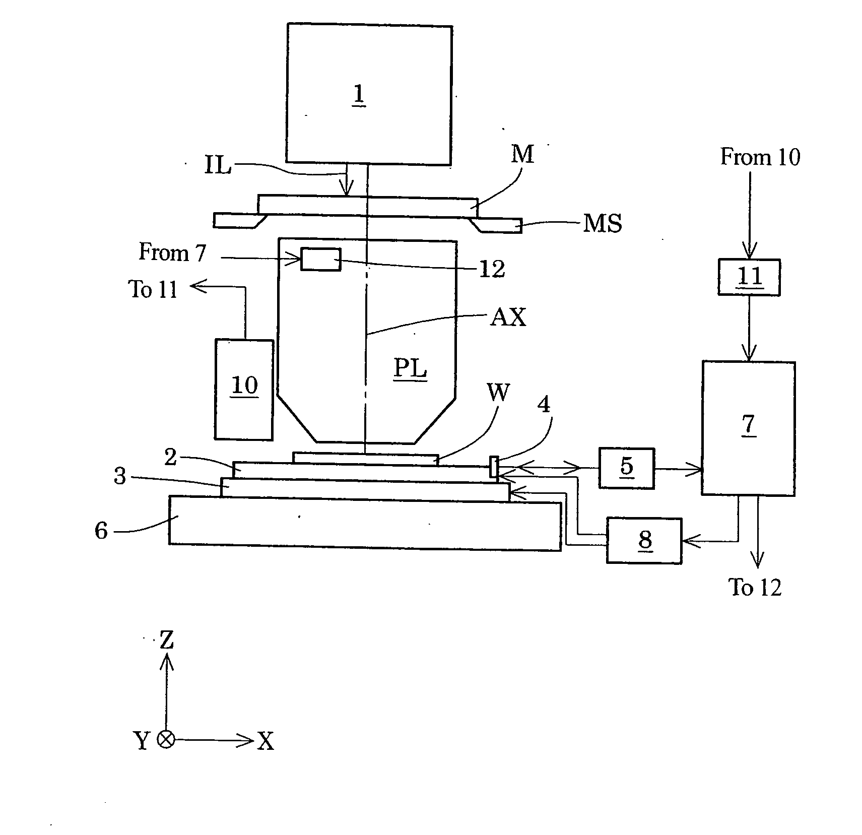
[0032]An embodiment of the present invention will now be described with reference to the drawings. FIG. 1 is a schematic diagram showing the structure of an exposure apparatus used when performing an exposure method according to the embodiment of the present invention. In FIG. 1, X-axis and Y-axis are orthogonal to each other within a plane parallel to a surface (exposure surface) of a wafer W, whereas the Z-axis extends in a direction normal to the surface of the wafer W. More specifically, the XY plane extends horizontally and the (+)Z-axis extends upward in the vertical direction.

[0033]The exposure apparatus shown in FIG. 1 includes an exposure light source, such as an ArF excimer laser, and an illumination unit 1, which includes an optical integrator (homogenizer), a field stop, and a condenser lens. The illumination unit 1 illuminates a mask (reticle) M, on which a pattern that is to be transferred is formed, with exposure light IL, which is emitted from the light source. The i...


PUM

PropertyMeasurementUnit
shapeaaaaaaaaaa
opticalaaaaaaaaaa
photosensitiveaaaaaaaaaa

Abstract

An exposure method enabling deformation occurring in a unit exposure field to be measured rapidly and accurately and enabling a plurality of patterns to be superimposed on a substrate with high accuracy. The exposure method of the present embodiment for exposing a bright-dark pattern on the substrate using a projection optical system includes a position detection process for detecting the positions of a plurality of position detection marks, relative to a substrate-in-plane-direction of the substrate, arranged in at least one functional element in a unit exposure field of the substrate, a deformation calculation process for calculating the state of deformation occurring in the unit exposure field based on information related to the positions of the position detection marks obtained in the position detection process, and a shape modification process for modifying the shape of the bright-dark pattern to be exposed on the substrate based on the deformation state obtained in the deformation calculation process.

Description

CROSS-REFERENCE TO RELATED APPLICATIONS[0001]This application claims the benefit of U.S. Provisional Patent Application No. 60 / 907,595, filed on Apr. 10, 2007.BACKGROUND OF THE INVENTION[0002]An embodiment of the present invention relates to an exposure method and an electronic device manufacturing method. More particularly, the embodiment of the present invention relates to an exposure method used in a lithography process for manufacturing electronic devices such as semiconductor devices, imaging devices, liquid crystal display devices, and thin-film magnetic heads.[0003]A plurality of layers of circuit patterns are formed on a wafer (or a substrate such as a glass plate), which is coated with a photosensitive material, in processes for manufacturing devices such as semiconductor devices. An exposure apparatus is required to align a mask, on which a pattern to be transferred (a transferred pattern) is formed, and the wafer, on which a circuit pattern has been formed. The exposure a...

Claims


Application Information

Patent Timeline
Patent Type & Authority Applications(United States)
IPC IPC(8): G03F7/20
CPCG03F7/70266G03F7/703G03F7/70425G03F7/70633G03F7/70783H01L2223/5448G03F9/7084G03F9/7088H01L23/544H01L2223/54453H01L2223/5446G03F9/7003H01L2924/0002H01L2924/00G03F7/70775
Inventor SHIRAISHI, NAOMASAINOUE, HIDEYA
Owner NIKON CORP
Why Eureka
Try Eureka