
Surface-treated electro-deposited copper foil and method for manufacturing the same

a technology surface treatment, which is applied in the field of surface-treated electro-deposited copper foil and electro-deposited copper foil, can solve the problems of low surface roughness, large cost and volume, and low profile performance of electro-deposited copper foil manufactured by the prior art, and achieves small waviness and low profil

Active Publication Date: 2009-02-19
MITSUI MINING & SMELTING CO LTD
View PDF8 Cites 27 Cited by
  • Summary
  • Abstract
  • Description
  • Claims
  • Application Information

AI Technical Summary

Benefits of technology

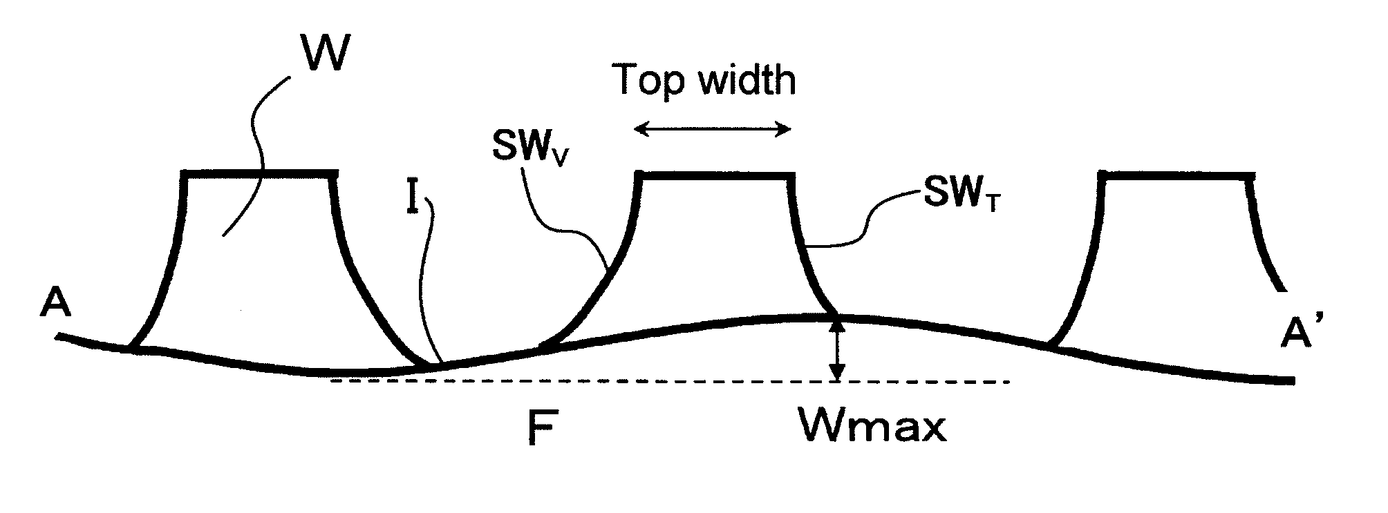
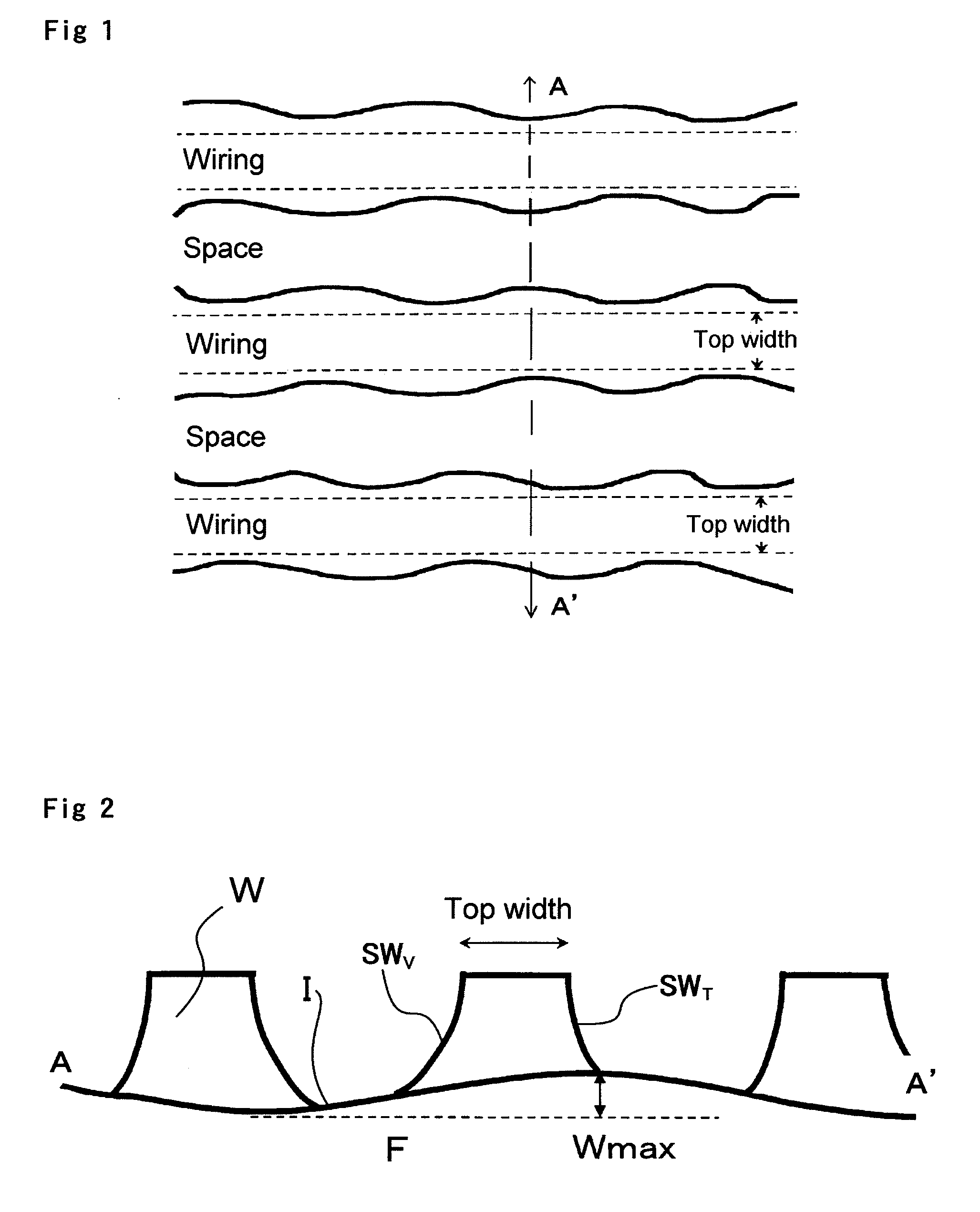
[0034]The surface-treated electro-deposited copper foil according to the present invention is an excellent low-profile surface-treated electro-deposited copper foil equal to or better than low-profile surface-treated electro-deposited copper foils that have conventionally been supplied to the market, and has a bonding surface having small waviness. Therefore, the surface-treated electro-deposited copper foil according to the present invention is suitable as material for forming the fine pitch wiring of a tape automated bonding (TAB) wiring board and / or a chip on film (COF) wiring board that has been remarkably required a low profile and small waviness for the bonding surface. The surface-treated electro-deposited copper foil according to the present invention is also suitable as a material for forming the electromagnetic wave shielding pattern in a plasma display panel.

Problems solved by technology

Further, it is also required to supply monitors at low cost and in a large amount.
When evaluation on 20 μm pitch wiring is carried out, even the electro-deposited copper foil manufactured by the prior art has low profile performance with excellent surface roughness, defects due to large waviness on the edge of wiring tends to occur in the formed fine pattern wiring.
Also, problems may occur in use for the electromagnetic shield for a plasma display panel where the formation of the same level of wiring is required.
For example, the resolution of the screen and the like do not satisfy the designed values, if the width of the wiring was not obtained as designed.

Method used


Image

  • Surface-treated electro-deposited copper foil and method for manufacturing the same
  • Surface-treated electro-deposited copper foil and method for manufacturing the same
  • Surface-treated electro-deposited copper foil and method for manufacturing the same

Examples


examples

Preparation of Electro-Deposited Copper Foils

[0090]In these Examples, seven types of electrolytic solutions in which the concentration of various additives was adjusted to the concentration described in Table 1 were used to prepare electro-deposited copper foils. Specifically, as a sulfuric acid base copper electrolytic solution, copper sulfate (reagent) and sulfuric acid (reagent) were dissolved in pure water to adjust copper concentration of 80 g / L and free sulfuric acid concentration of 140 g / L to obtain a base solution. To the base solution, MPS-Na or SPS-Na as a sulfonate of an active sulfur compound, three types of DDAC polymers as quaternary ammonium salt polymers having a cyclic structure (UNISENCE FPA100L, FPA101L, and FPA102L manufactured by SENKA CORPORATION), and hydrochloric acid were added. The molecular weight of the DDAC polymers used satisfies FPA100L<FPA101L<FPA102L.

TABLE 1Additive concentration (ppm)A sulfonate of activesulfur compoundDDAC polymer / ExampleMPS-NaSPS...


PUM

PropertyMeasurementUnit
waviness heightaaaaaaaaaa
surface roughnessaaaaaaaaaa
peak to valley heightaaaaaaaaaa

Abstract

It is an object to provide a surface-treated electro-deposited copper foil which has a low profile at a level equal to or excellent than that of low-profile surface-treated electro-deposited copper foils that have conventionally been supplied to the market and in which waviness affecting the straight line performance of wiring is small, and a method for manufacturing the same. In order to achieve this object, in the surface-treated electro-deposited copper foil, the maximum waviness height (Wmax) of the bonding surface to be bonded with an insulation layer-constituting material to be 0.05 μm to 0.7 μm, the maximum peak to valley height (PV) to be 0.05 to 1.5 μm, and the surface roughness (Rzjis) to be 0.1 μm to 1.0 μm. The electro-deposited copper foil used for the manufacturing of this surface-treated electro-deposited copper foil is manufactured by using a sulfuric acid base copper electrolytic solution obtained by adding 3-mercapto-1-propanesulfonic acid or bis(3-sulfopropyl)disulfide, a quaternary ammonium salt polymer having a cyclic structure, and chlorine, and using a cathode having small surface roughness, under electrolysis conditions of carrying out continuous first-step electrolysis to n-th-step electrolysis at two or more different levels of electric current density.

Description

TECHNICAL FIELD[0001]The present invention relates to a surface-treated electro-deposited copper foil, an electro-deposited copper foil, and a method for manufacturing the same, as well as a rigid copper clad laminate, a rigid printed wiring board, a flexible copper clad laminate, and a flexible printed wiring board using the surface-treated electro-deposited copper foil. Particularly, the present invention relates to a surface-treated electro-deposited copper foil having a bonding surface, to be bonded with an insulation layer-forming material, having small waviness that is excellent in fine pattern wiring forming performance when used for a printed wiring board and the like, and to a method for manufacturing the same.BACKGROUND ART[0002]An electro-deposited copper foil is widely used as the base material of a printed wiring board because metal copper is good in electric conductivity, is relatively cheap, and is easy in handling also. The so-called downsizing, such as miniaturizati...

Claims


Application Information

Patent Timeline
Patent Type & Authority Applications(United States)
IPC IPC(8): B32B3/00B21C37/02C25D5/00
CPCC25D1/04Y10T428/12903C25D5/16C25D5/18C25D5/48C25D7/06H05K3/384H05K2201/0355H05K2203/0307H05K2203/0723H05K2203/1476Y10T428/24917Y10T428/24355Y10T428/12472Y10T428/12993Y10T428/12882Y10T428/12438Y10T428/12451C25D3/38C25D5/605C25D5/617C25D5/627B32B15/08H05K1/09
Inventor DOBASHI, MAKOTOMATSUDA, MITSUYOSHITOMONAGA, SAKIKOSAKAI, HISAOSAKATA, TOMOHIROYOSHIOKA, JUNSHINISHIKAWA, JOTAGUCHI, TAKEO
Owner MITSUI MINING & SMELTING CO LTD
Learn More