Solid-state image capturing device, manufacturing method for the solid-state image capturing device, and electronic information device
- Summary
- Abstract
- Description
- Claims
- Application Information
AI Technical Summary
Benefits of technology
Problems solved by technology
Method used
Image
Examples
embodiment 1
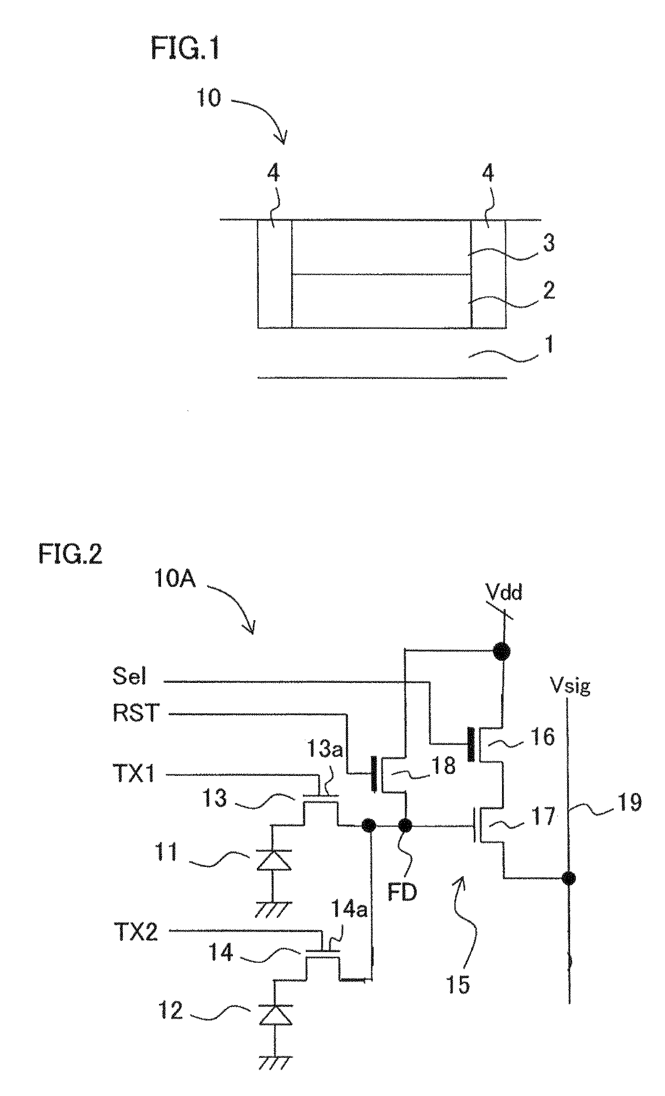
[0097]FIG. 1 is a longitudinal cross sectional view schematically showing a structural principle of a unit pixel in a solid-state image capturing device according to Embodiment 1 of the present invention.
[0098]According to FIG. 1, in a light receiving section (photoelectric conversion section) in an unit pixel 10 of the solid-state image capturing device according to Embodiment 1, a low concentration opposite conductivity layer 2 is provided on a single conductivity substrate or single conductivity layer 1. On the low concentration opposite conductivity layer 2, a high concentration opposite conductivity layer 3 having a higher impurity concentration than that of the low concentration opposite conductivity layer 2 is provided, and a photodiode is formed deep inside the substrate by a PN junction of the single conductivity layer 1 and the low concentration opposite conductivity layer 2.
[0099]As described above, by providing the low concentration opposite conductivity layer 2 having a...
embodiment 2
[0102]FIG. 2 is a circuit diagram showing a unit pixel of a solid-state image capturing device having a two pixel shared structure in a CMOS image sensor according to Embodiment 2 of the present invention.
[0103]According to FIG. 2, in a unit pixel section 10A in the solid-state image capturing device having a two pixel shared structure in a CMOS image sensor according to Embodiment 2, photodiodes 11 and 12 functioning as two light receiving sections and two transfer transistors 13 and 14 for reading out a signal charge corresponding to the respective photodiodes 11 and 12 are provided, and one common signal readout circuit 15 is also provided for the two photodiodes and two transfer transistors.
[0104]The readout circuit 15 includes a selection transistor 16 as a pixel selection section, an amplifying transistor 17 for amplifying a signal in accordance with a signal charge voltage of a floating diffusion FD of a selected pixel, connected in series to the selection transistor 16 and f...
embodiment 3
[0139]FIG. 8 is a longitudinal cross sectional view schematically showing a unit pixel of a solid-state image capturing device in a CCD image sensor according to Embodiment 3 of the present invention.
[0140]In FIG. 8, a low concentration P-type well 32 is provided on a substrate section of an N-type semiconductor substrate 31 in each unit pixel 10B of a CCD image sensor according to Embodiment 3. A P-type layer 33 having a higher concentration than the low concentration P-type well 32 is provided on the low concentration P-type well 32. In addition, a low concentration N-layer 34 functioning as a low concentration opposite conductivity layer is provided for every light receiving region in a plan view in the low concentration P-type well 32 and the high concentration P-type layer 33. A high concentration N-layer 35 is provided on the low concentration N-layer 34, the high concentration N-layer 35 functioning as a high concentration opposite conductivity layer and having a higher impur...
PUM
 Abstract
Description
Claims
Application Information


