Semiconductor device having diode-built-in IGBT and semiconductor device having diode-built-in DMOS

a semiconductor device and diode element technology, which is applied in the direction of logic circuits using specific components, logic circuits using semiconductor devices, pulse techniques, etc., can solve the problems of increasing forward voltage vf of the diode elements, increasing forward loss caused by the diode elements, and reducing the efficiency of the diode. , to achieve the effect of suppressing the increase in forward loss caused by the fwd diod

Active Publication Date: 2009-03-05
DENSO CORP
View PDF29 Cites 102 Cited by
  • Summary
  • Abstract
  • Description
  • Claims
  • Application Information

AI Technical Summary

Benefits of technology

[0014]In the above semiconductor device the interference of the action of the diode with the action of the IGBT can be avoided. Further, since the diode and IGBT are simultaneously turned on, an increase in a loss in the forward voltage of the diode can be prevented.
[0026]In the above device, an increase in a forward loss caused by the FWD diode can be effectively suppressed.

Problems solved by technology

Consequently, the body diode including the diode elements cannot readily act in a forward direction due to the gate potential of the IGBT elements.
As a result, the forward voltage Vf of the diode elements increases, and the forward loss caused by the diode elements increases.
This poses a problem in that the circuit scale gets larger.
This poses a problem in that the cost of the control IC increases.
However, since the current detection elements having such a structure are affected by a gate potential, a current cannot readily flow into the current detection elements.
In other words, feedback cannot be precisely performed, and an increase in a forward loss caused by the commutation diode elements cannot be effectively suppressed.

Method used


Image

  • Semiconductor device having diode-built-in IGBT and semiconductor device having diode-built-in DMOS
  • Semiconductor device having diode-built-in IGBT and semiconductor device having diode-built-in DMOS
  • Semiconductor device having diode-built-in IGBT and semiconductor device having diode-built-in DMOS

Examples


first embodiment

[0060]A first embodiment of the present disclosure will be described below with reference to the drawings. A semiconductor device of the present embodiment is used as a power switching device (which may be called an insulated-gate bipolar transistor (IGBT) device with a body diode) to be incorporated in an inverter module for electric and hybrid vehicles (EHVs).

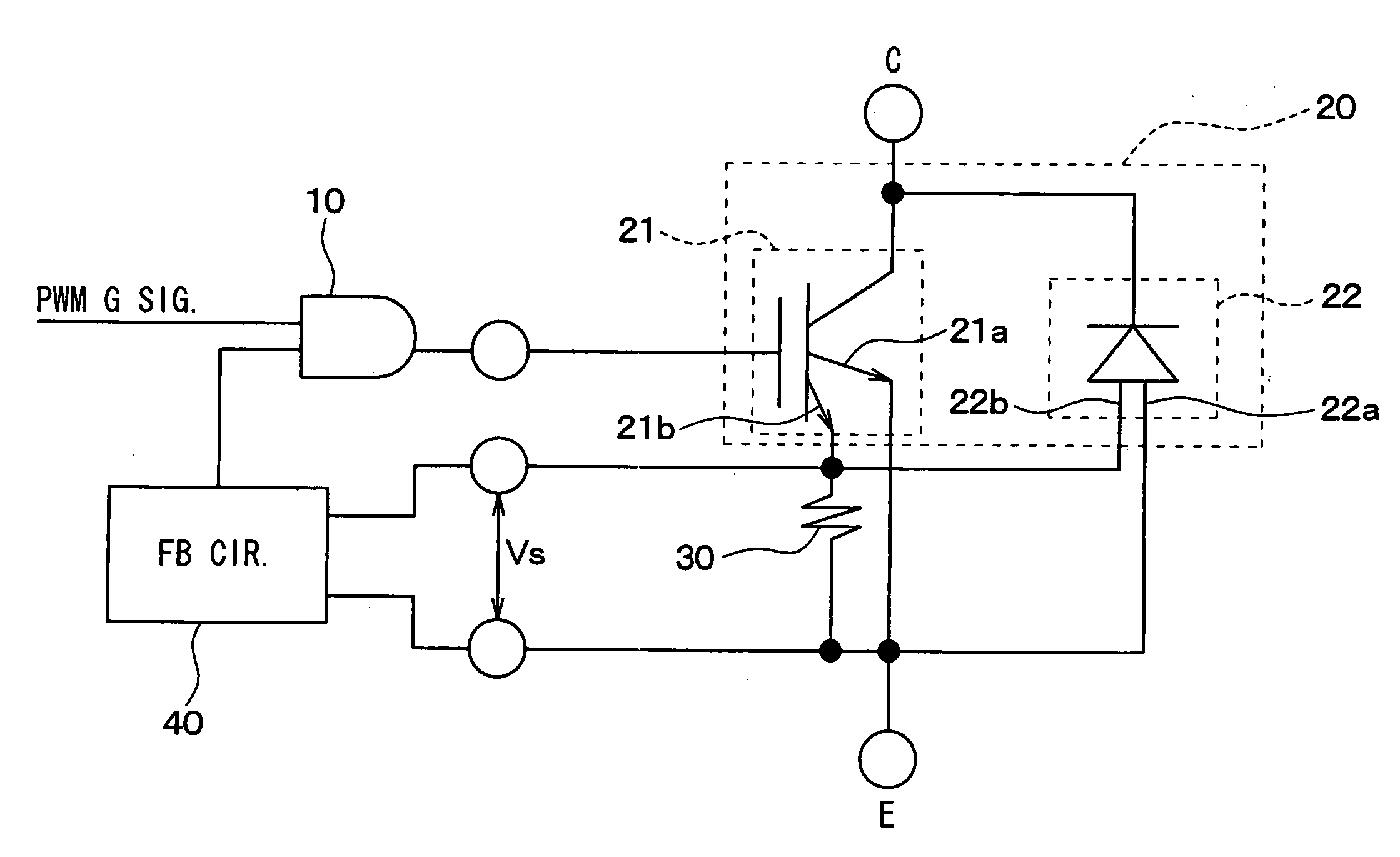
[0061]FIG. 1 is a circuit diagram of the semiconductor device in accordance with the present embodiment. As shown in the drawing, the semiconductor device includes an AND circuit 10, an IGBT 20 with a body diode, a sense resistor 30, and a feedback circuit 40.

[0062]The AND circuit 10 is a logic circuit that when all inputted signals have a high level, outputs a high-level signal, and is a so-called AND gate. An external pulse-width-modulated (PWM) gate signal with which the IGBT 20 with a body diode is driven, and an output of the feedback circuit 40 are inputted to the AND circuit 10. Incidentally, the PWM gate signal is pro...

second embodiment

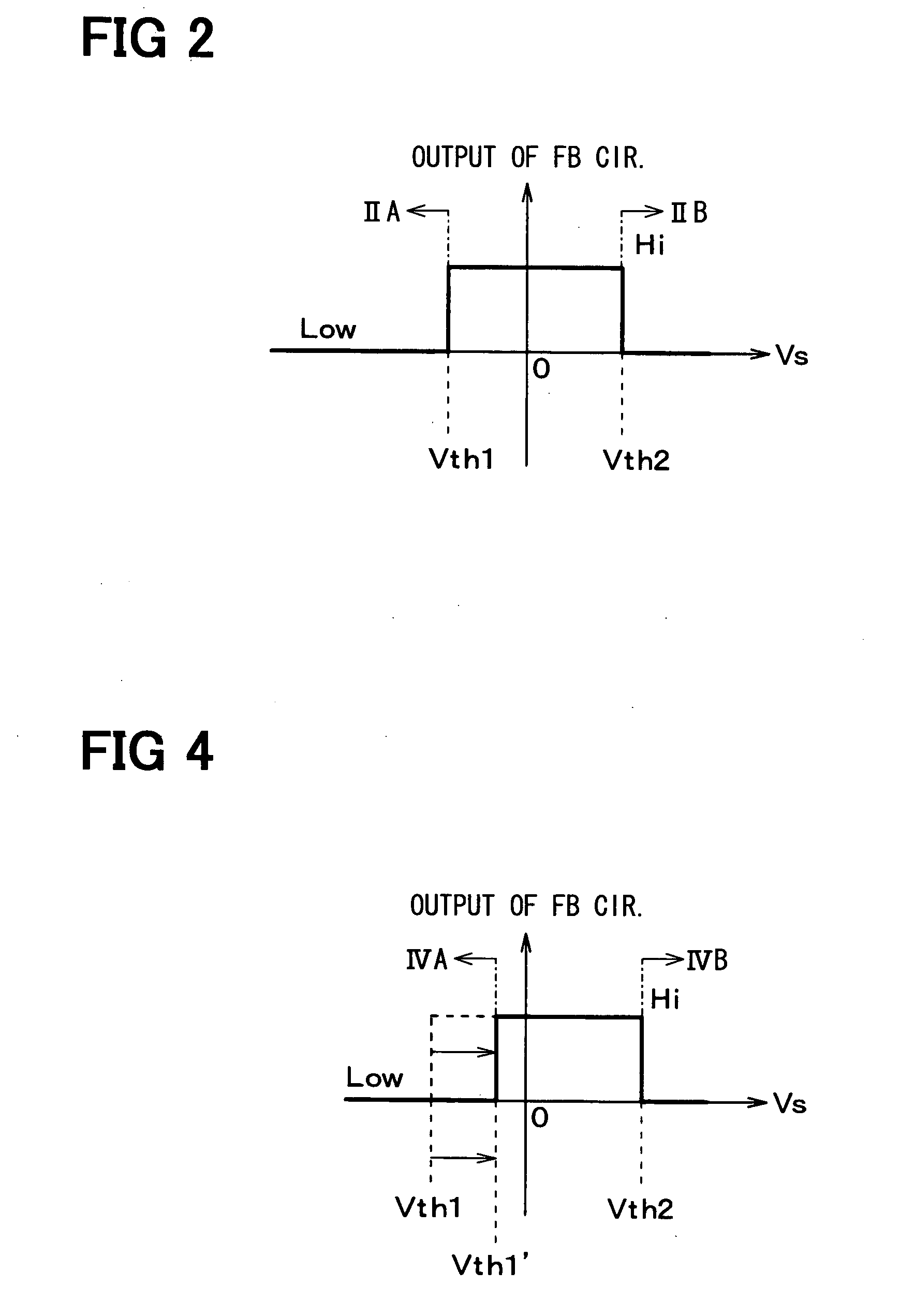
[0090]In the present embodiment, the temperature of a semiconductor device is detected, and the diode current sensing threshold Vth1 is changed to another on the basis of the detected temperature.

[0091]FIG. 3 is a circuit diagram of a semiconductor device in accordance with the present embodiment. As shown in the drawing, the semiconductor device in accordance with the present embodiment has temperature sensitive diode elements 50 added to the construction shown in FIG. 1.

[0092]The temperature sensitive diode elements 50 are used to measure the temperature of the semiconductor device, or more particularly, the temperature of the IGBT 20 with a body diode. The temperature sensitive diode elements 50 output temperature-dependent voltages, that is, have the forward voltages thereof varied, and output forward voltages dependent on heat dissipated along with the action of the IGBT 20 with a body diode.

[0093]The temperature sensitive diode elements 50 are constructed by, for example, form...

third embodiment

[0104]In the second embodiment, the components are constructed as independent parts. In the present embodiment, the components of the second embodiment are integrated into one chip.

[0105]FIG. 5A is an overall illustrative diagram of a semiconductor chip 60 in accordance with the present embodiment. FIG. 5B is a circuit diagram of a circuit included in the semiconductor chip 60 and is identical to the circuit diagram of FIG. 3. As shown in FIG. 5A, the semiconductor chip 60 includes an IGBT 20 with a body diode, temperature sensitive diode elements 50, a processing circuit unit 70, current sensing elements 61, a gate pad 62, and a guard ring 63.

[0106]The processing circuit unit 70 shown in FIG. 5A includes a feedback circuit 40, an AND circuit 10, and a sense resistor 30 which are shown in FIG. 5B. The feedback circuit 40 is formed with, for example, a thin-film transistor circuit.

[0107]Moreover, the current sensing elements 61 sense currents that flow into IGBT elements 21a and diod...


PUM


Abstract

A semiconductor device includes: a semiconductor substrate; a diode-built-in insulated-gate bipolar transistor having an insulated-gate bipolar transistor and a diode, which are disposed in the substrate, wherein the insulated-gate bipolar transistor includes a gate, and is driven with a driving signal input into the gate; and a feedback unit for detecting current passing through the diode. The driving signal is input from an external unit into the feedback unit. The feedback unit passes the driving signal to the gate of the insulated-gate bipolar transistor when the feedback unit detects no current through the diode, and the feedback unit stops passing the driving signal to the gate of the insulated-gate bipolar transistor when the feedback unit detects the current through the diode.

Description

CROSS REFERENCE TO RELATED APPLICATIONS[0001]This application is based on Japanese Patent Applications No. 2007-229959 filed on Sep. 5, 2007, No. 2007-268328 filed on Oct. 15, 2007, No. 2008-96017 filed on Apr. 2, 2008 and No. 2008-96018 filed on Apr. 2, 2008, the disclosures of which are incorporated herein by reference.FIELD OF THE INVENTION[0002]The present invention relates to a semiconductor device having a diode-built-in IGBT, and a semiconductor device having a diode-built-in DMOS.BACKGROUND OF THE INVENTION[0003]In the past, a proposal has been made of an IGBT with a body diode that has diode elements and IGBT elements formed in the same semiconductor substrate (refer to, for example, a patent document 1, that is, IP-A-6-351226 corresponding to U.S. Pat. No. 5,559,656). The IGBT with a body diode has the anode electrodes of the diode elements and the emitter electrodes of the IBGT elements formed in common with each other, and has the cathode electrodes of the diode elements...

Claims


Application Information

Patent Timeline
Patent Type & Authority Applications(United States)
IPC IPC(8): H01L29/739
CPCH01L29/7397H03K17/0828H03K17/145H03K2217/0027H01L2924/0002H01L27/0255H01L2924/00H02M1/32H02M1/0009
Inventor KOUNO, KENJI
Owner DENSO CORP
Why Eureka
Try Eureka