Semiconductor fabrication system, and flow rate correction method and program for semiconductor fabrication system

a technology of semiconductor fabrication and flow rate correction, which is applied in the direction of process and machine control, semiconductor/solid-state device testing/measurement, instruments, etc., can solve the problems of deviation of actual flow rate and mfc from the set flow rate, and achieve accurate detection and correction, and accurate detection and correction.

Inactive Publication Date: 2009-03-05
TOKYO ELECTRON LTD
View PDF3 Cites 19 Cited by
  • Summary
  • Abstract
  • Description
  • Claims
  • Application Information

AI Technical Summary

Benefits of technology

[0036]In accordance with the above program, it is possible to perform a flow rate control capable of accurately detecting and correcting the first zero point shift due to the use of the flow rate controller in a state where the effect of the second zero shift does not exist, and accurately detecting and correcting the second zero point shift due to the thermal siphon effect in a state where the effect of the second zero shift does not exist.
[0037]In accordance with the present invention, the amount of the zero point shift due to the thermal siphon effect, which actually occurs during the substrate process, can be accurately detected and properly corrected. Therefore, the accuracy of controlling the flow rate is greatly improved without depending on the installation arrangement of the flow rate controller. Furthermore, the amount of the zero point shift due to the thermal siphon effect is accurately detected to be corrected without depending on the configuration of the flow rate controller.

Problems solved by technology

However, while the MFC is being used, an actual flow rate (i.e., a flow rate of a gas which actually passes through the MFC) may be deviated from the set flow rate, due to contamination (caused by corrosion or remaining products) in a pipe around which the flow rate sensors are wound.
For example, even when the actual flow rate is zero, a detected voltage value corresponding to the flow rate detected by the flow rate sensor is in many cases not zero, resulting in an error with slight deviation (see, e.g. Patent Document 1).

Method used


Image

  • Semiconductor fabrication system, and flow rate correction method and program for semiconductor fabrication system
  • Semiconductor fabrication system, and flow rate correction method and program for semiconductor fabrication system
  • Semiconductor fabrication system, and flow rate correction method and program for semiconductor fabrication system

Examples


first embodiment

Example of Configuration of Semiconductor Fabrication Apparatus in accordance with First Embodiment

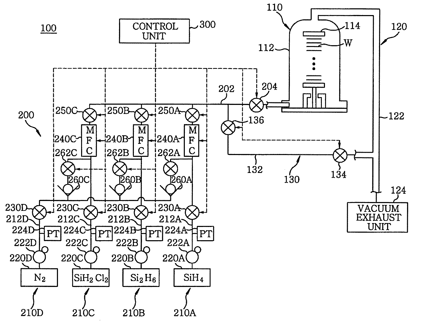
[0102]A semiconductor fabrication apparatus in accordance with a first embodiment of the present invention will be described with reference to the drawings. As an example of the semiconductor fabrication apparatus, a heat treatment apparatus for performing a specific heat treatment on a substrate, for example, a semiconductor wafer (hereinafter, referred to as a “wafer”), will be described. FIG. 1 shows an example of the configuration of the heat treatment apparatus in accordance with the first embodiment. The heat treatment apparatus 100 includes a heat treatment unit 110 as a processing unit for performing a process (for example, heat treatment) on the wafer W. The heat treatment unit 110 includes a bell-shaped reaction tube 112 having, for example, a reaction container (process container) or a reaction chamber (process chamber) shown in FIG. 1. A holding unit 114 loading a plurality...

second embodiment

Example of Configuration of Semiconductor Fabrication Apparatus of Second Embodiment

[0193]A semiconductor fabrication apparatus in accordance with a second embodiment of the present invention will be described with reference to the drawings. Like the above description of the first embodiment, a heat treatment apparatus for performing a specific heat treatment on a wafer will be described as an example of the semiconductor fabrication apparatus in accordance with the second embodiment. FIG. 12 illustrates an example of the configuration of the heat treatment apparatus 100 in accordance with the second embodiment. The heat treatment apparatus 100 in accordance with the second embodiment is different from the heat treatment apparatus in accordance with the first embodiment in the configuration of the gas supply system 200. Specifically, in the heat treatment apparatus 100 in accordance with the first embodiment, the first, second and third MFCs 240A, 240B and 240C are configured to con...


PUM

PropertyMeasurementUnit
output voltageaaaaaaaaaa
timeaaaaaaaaaa
semiconductoraaaaaaaaaa

Abstract

Zero point shift based on thermal siphon effect occurring actually when a substrate is processed is detected accurately and corrected suitably. The semiconductor fabrication system comprises a gas supply passage (210) for supplying gas into a heat treatment unit (110), an MFC (240) for comparing an output voltage from a detecting unit for detecting the gas flow rate of the gas supply passage with a set voltage corresponding to a preset flow rate and controlling the gas flow rate of the gas supply passage to the set flow rate, and a control unit (300). The control unit replaces gas in the MFC by gas which is to be used at least for processing a substrate before the substrate is processed, detects the output voltage from the MFC under a state where valves (230, 250) provided in the upstream and the downstream of the MFC are closed and stores the detected output voltage in a storage unit, corrects the set voltage corresponding to the flow rate of gas to be used for processing the substrate based on the output voltage from the MFC stored in the storage unit at the time of processing the substrate, and sets the corrected set voltage in the MFC.

Description

FIELD OF THE INVENTION[0001]The present invention relates to a semiconductor fabrication apparatus which controls a flow rate of gas or liquid by using a flow rate controller, such as a mass flow controller, and performs a specific process on a substrate; a method of correcting the flow rate; and a program therefor.BACKGROUND OF THE INVENTION[0002]Conventionally, in a semiconductor device manufacturing process (e.g., a film formation process using a film forming gas, an etching process using an etching gas, and the like), a gas or a liquid is supplied to a semiconductor fabrication apparatus. In this case, a flow rate of the gas or liquid is controlled by a flow rate controller such as a mass flow controller (MFC) installed in a supply flow path through which the gas or liquid is supplied.[0003]The MFC is generally configured to split the supply flow path into a lateral flow path and a main flow path running in parallel. The lateral flow path includes an upstream sensor and a downst...

Claims


Application Information

Patent Timeline
Patent Type & Authority Applications(United States)
IPC IPC(8): H01L21/66H01L21/306H01L21/30
CPCC23C16/455G05D7/0658C23C16/52C23C16/45561G01F1/00G05D7/06H01L21/02
Inventor MORIYA, SHUJIOKABE, TSUNEYUKIEBI, HIROYUKISHIMIZU, TETSUOKITAGAWA, HITOSHI
Owner TOKYO ELECTRON LTD
Why Eureka
Try Eureka