Light-emitting device using oxide semiconductor thin-film transistor and image display apparatus using the same
a technology of semiconductor thin-film transistors and light-emitting devices, which is applied in the direction of static indicating devices, discharge tubes luminescnet screens, instruments, etc., can solve the problems of significant reduction of device structure and use of design in the device structure, and unstable operation of
- Summary
- Abstract
- Description
- Claims
- Application Information
AI Technical Summary
Benefits of technology
Problems solved by technology
Method used
Image

Examples
example 1
[0077]In this example, experiments for spectral sensitivity measurement were performed on the amorphous oxide used in the present invention.
[0078]First, an amorphous In—Ga—Zn oxide was formed on a substrate by a sputtering method. Specifically, the amorphous oxide was deposited in a thickness of 50 nm on a glass substrate (Corning 1737 glass produced by Corning Incorporated) by a high-frequency sputtering method under an atmosphere containing a gas mixture of oxygen and argon. A sintered body of In:Ga:Zn=1:1:1 was used as a target material. The reached vacuum degree in a growth chamber was 8×10⁻⁴ Pa. The total pressure of oxygen and argon was 5.3×10⁻¹ Pa. The oxygen partial pressure was 1.8×10⁻² Pa.
[0079]A substrate temperature was not particularly set and thus film formation was performed without heating. The room temperature during the film formation was approximately 25° C. An X-ray was made incident on obtained films at an incident angle of 0.5 degrees relative to the film surfa...
example 2
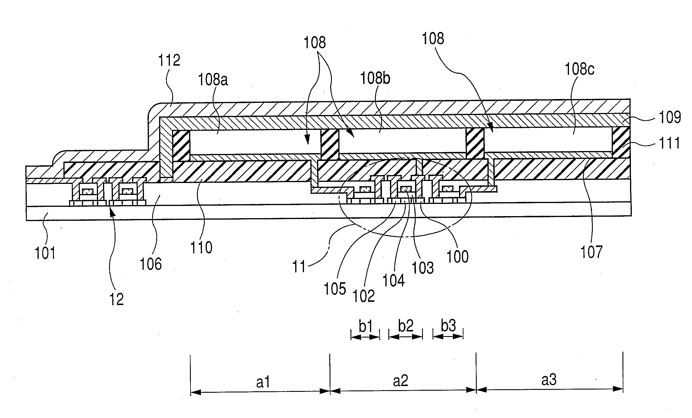
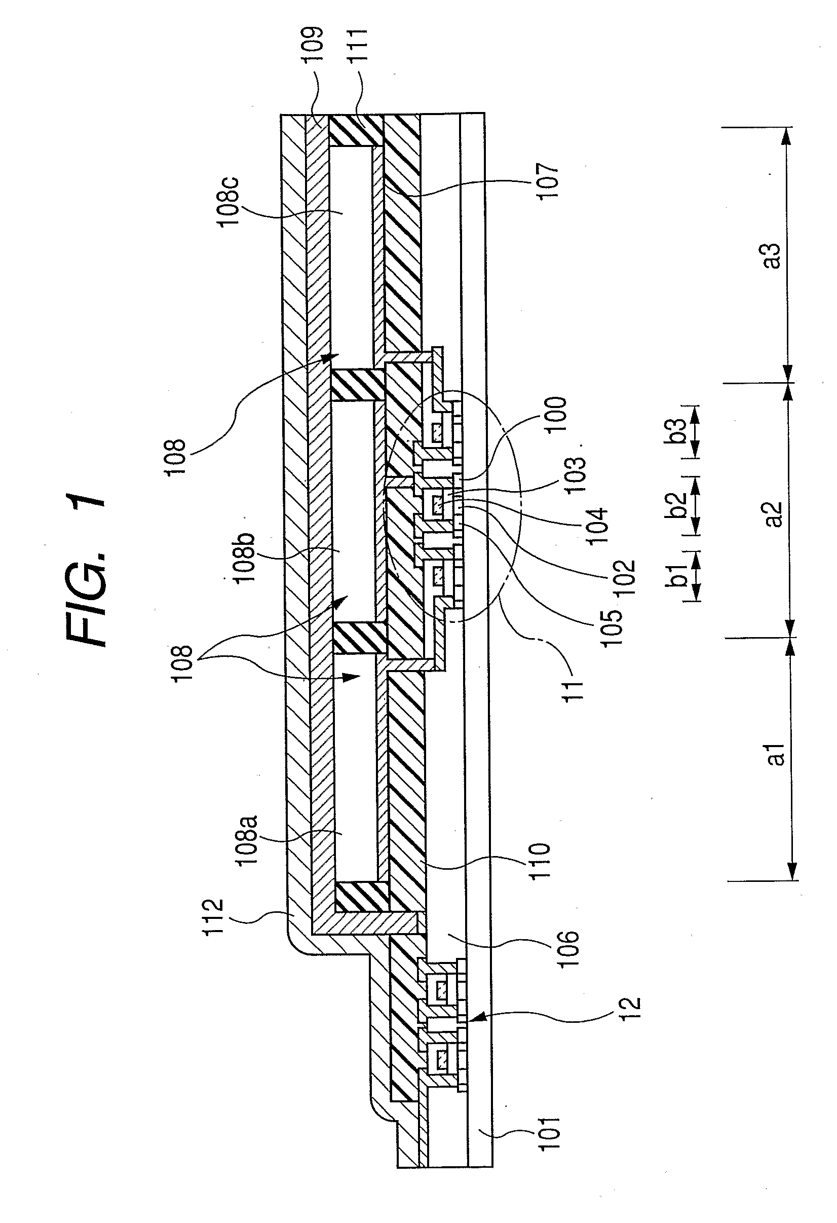
[0085]In this example, as shown in FIG. 7, a stagger (top-gate) metal-insulator-semiconductor field effect transistor (MISFET) device was manufactured.
[0086]First, a metal film was formed in a thickness of 30 nm on the glass substrate 1. The drain terminal 4 and the source terminal 3 were formed by a photolithography method and a lift-off method, and then an amorphous film (IGZO) which was used as the channel layer (active layer) 2 and had a metal composition ratio In:Ga:Zn=1.00:0.94:0.65 was formed thereon in a thickness of 30 nm by a sputtering method. An amorphous oxide film formation condition was the same as the condition of the evaluation experiments. Finally, a Y2O3 film used as the gate insulating film 5 was formed by an electron beam deposition method, a metal (Au) film was formed thereon, and the gate terminal 6 was formed by a photolithography method and a lift-off method.
[0087]The I-V characteristics of the MISFET device were evaluated during the irradiation of different...
example 3
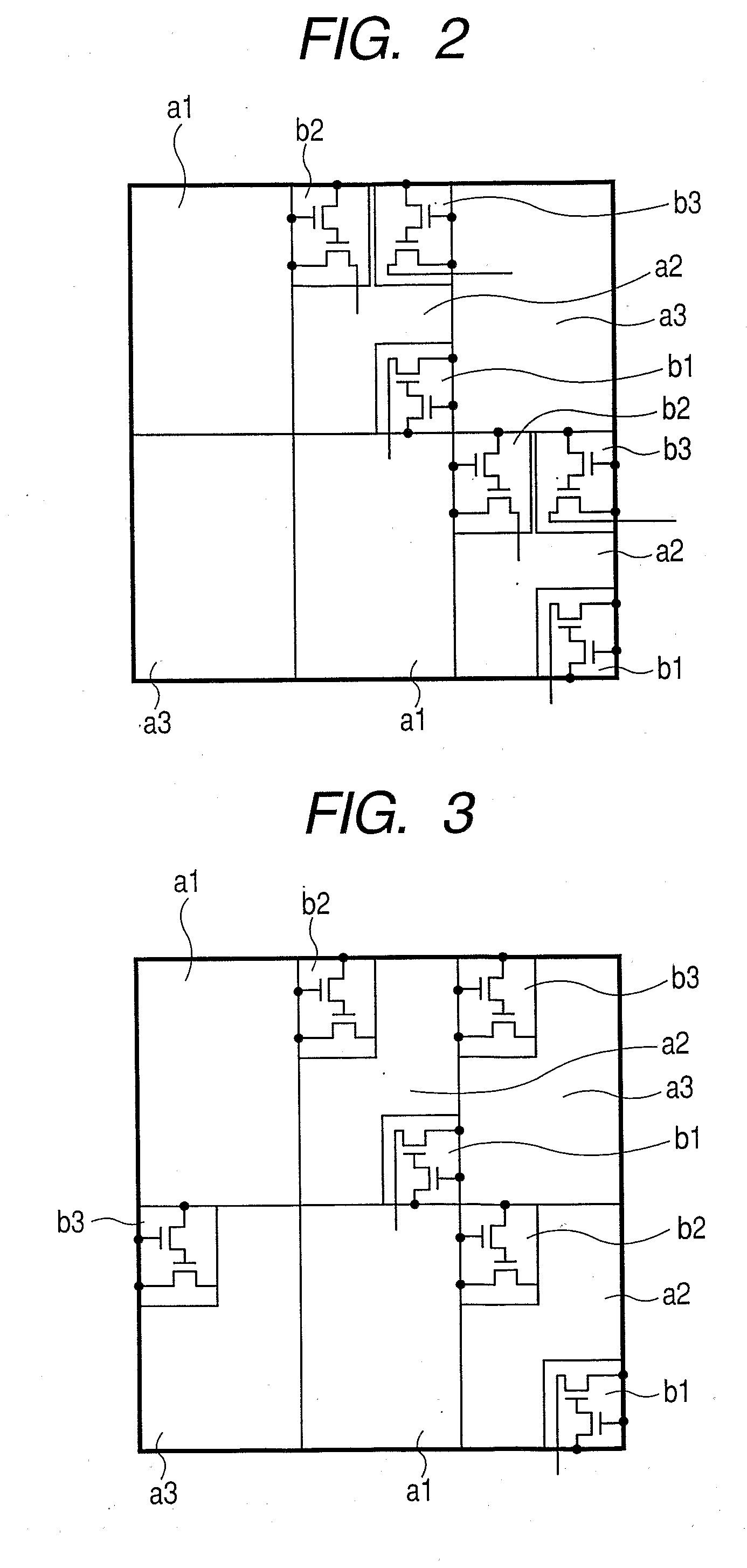
[0090]In this example, a light-emitting device in which TFTs were arranged in the red pixel region is manufactured.
[0091]First, MISFET devices were formed by substantially the same method as the method used in Example 2. In a series of processes, each layer was formed at a desirable size by a photolithography method and a lift-off method. At this time, TFTs were arranged in the red pixel region as in the case shown in FIG. 2. Then, an insulating layer was formed by the same method and contact holes for a drain electrode were formed therein.
[0092]After that, an ITO film was formed in a thickness of 300 nm by a sputtering method to obtain a lower electrode. At this time, drain electrodes were connected with the lower electrode through the contact holes to form wirings. Next, a hole injection layer was formed in a thickness of 60 nm by a resistance evaporation method, and a hole transport layer was formed thereon in a thickness of 20 nm. Then, each of light-emitting layers of red, blue...
PUM
 Abstract
Description
Claims
Application Information
 - Generate Ideas
- Intellectual Property
- Life Sciences
- Materials
- Tech Scout
- Unparalleled Data Quality
- Higher Quality Content
- 60% Fewer Hallucinations
Browse by: Latest US Patents, China's latest patents, Technical Efficacy Thesaurus, Application Domain, Technology Topic, Popular Technical Reports.
© 2025 PatSnap. All rights reserved.Legal|Privacy policy|Modern Slavery Act Transparency Statement|Sitemap|About US| Contact US: help@patsnap.com