Spin-on antireflective coating for integration of patternable dielectric materials and interconnect structures

Inactive Publication Date: 2009-03-26
GLOBALFOUNDRIES US INC
View PDF77 Cites 71 Cited by
  • Summary
  • Abstract
  • Description
  • Claims
  • Application Information

AI Technical Summary

Benefits of technology

[0068]This patternable low-k/inorganic ARC method of present invention dramatically reduces the complexity in the fabrication of current interconnect structures. The photoresist used in the prior art integration is no longer needed. In addition to not requiring a separate photoresist, the present invention also does not utilize a plasma etching

Problems solved by technology

Unfortunately, conventional organic antireflective coatings are generally not suitable for the lithography of a patternable low-k material as the antireflective coating layer is a permanent part of the interconnect stru

Method used


Image

  • Spin-on antireflective coating for integration of patternable dielectric materials and interconnect structures
  • Spin-on antireflective coating for integration of patternable dielectric materials and interconnect structures
  • Spin-on antireflective coating for integration of patternable dielectric materials and interconnect structures

Examples


example 1

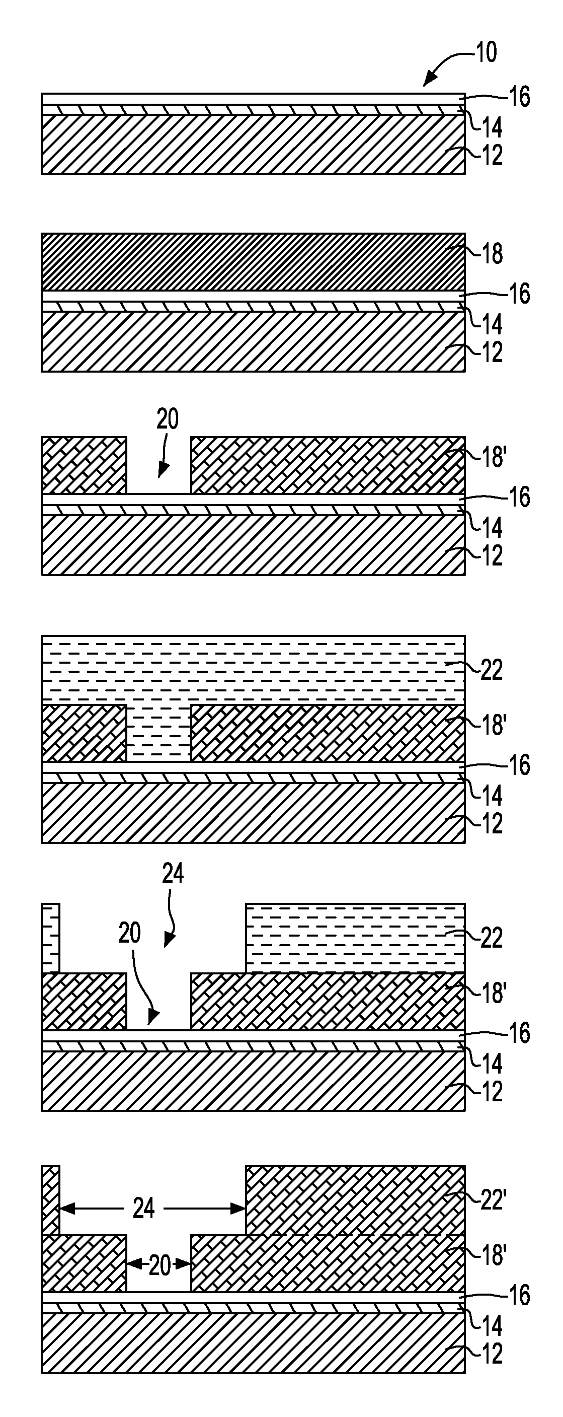
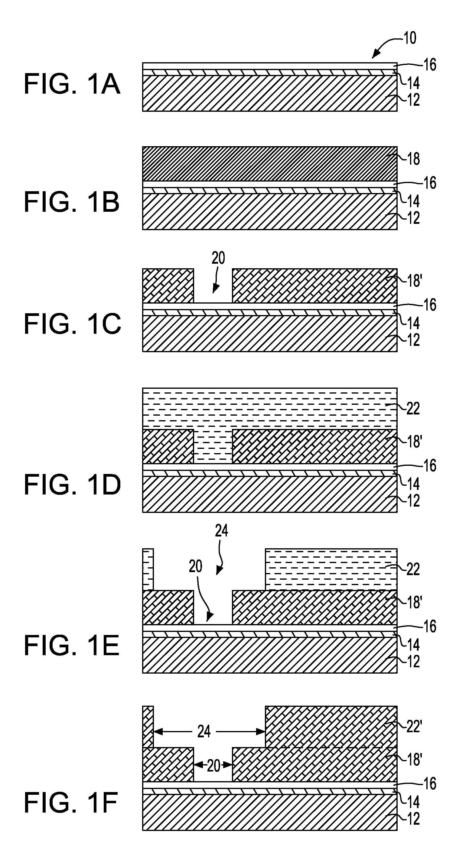
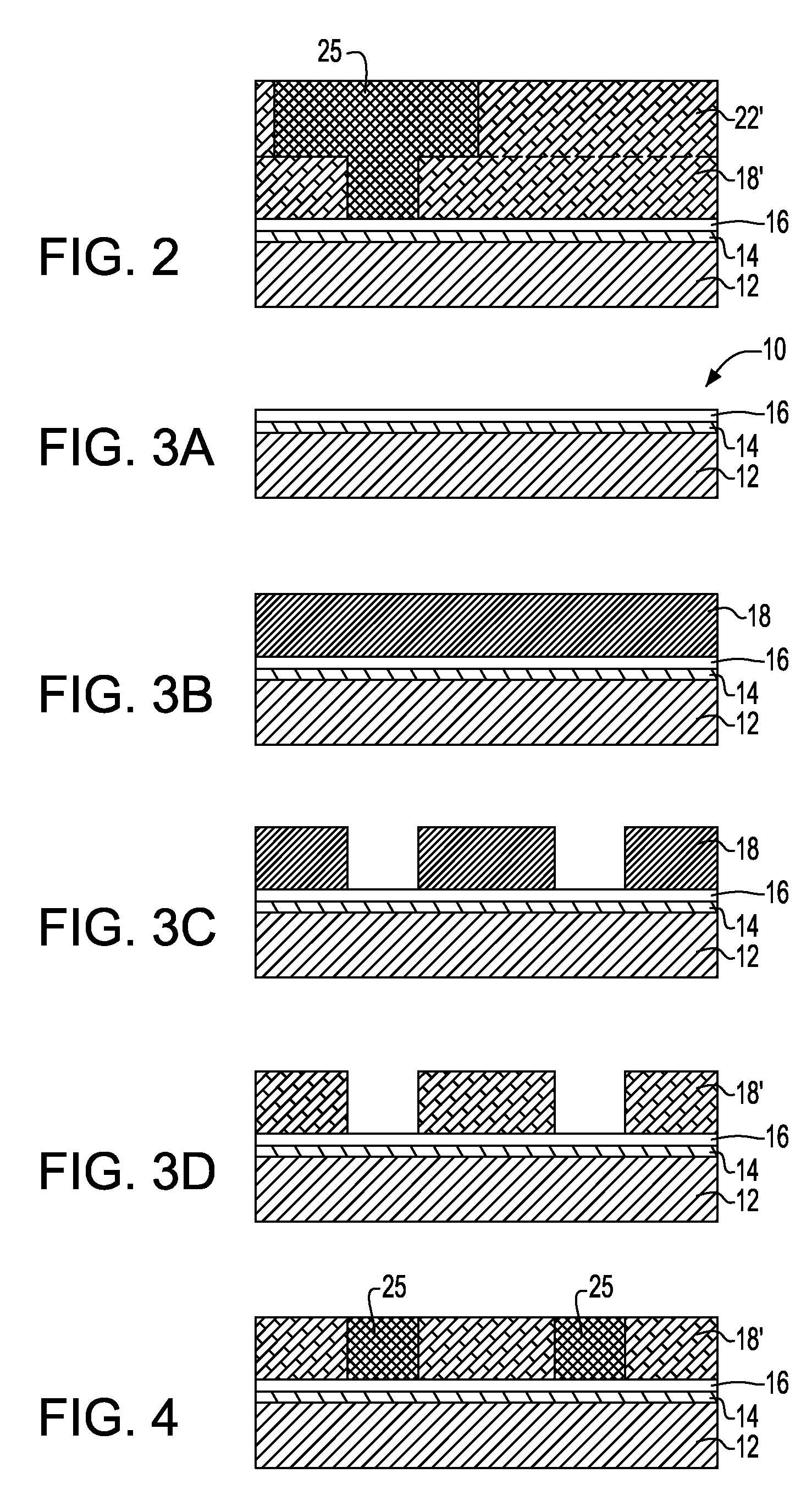
Single-Damascene Integration of Negative-Tone Patternable Low-k Dielectric (k=2.7) On-Chip Electrical Insulator

example 1a

Inorganic Spin-On Antireflective Layer for Patternable Low-k Resist-1 (PPLKARC01)

[0175]An inorganic spin-on antireflective coating composition was formulated with the following components: 1.5 g of 9-anthracenemethanol bounded poly(4-hydroxybenzylsilsesquioxane) with 20% of 9-anthracenemethanol, 0.176 g of glycoluril resin (POWDERLINK cross-linking agent), 0.088 g of K-Pure 2678 (thermal acid generator from King Industry), 0.1 g of FC430 surfactant (10 wt % PGMEA solution sold by 3M Corporation) and 33.429 g of propylene glycol monomethyl ether acetate (PGMEA) to form a solution with a 5 wt. % of total solid content. The resulting formulation was filtered through a 0.2 micron filter.

example 1b

Inorganic spin-On Antireflective Layer for Patternable Low-k Resist-2 (PPLKARC02)

[0176]An inorganic spin-on antireflective coating composition was formulated with the following components: 1.5 g of 9-anthracenemethanol bounded poly(4-hydroxybenzylsilsesquioxane) with 15% of 9-anthracenemethanol, 0.176 g of glycoluril resin (POWDERLINK cross-linking agent), 0.088 g of K-Pure 2678 (thermal acid generator from King Industry), 0.1 g of FC430 surfactant (10 wt % PGMEA solution sold by 3M Corporation) and 33.429 g of propylene glycol monomethyl ether acetate (PGMEA) to form a solution with a 5 wt. % of total solid content. The resulting formulation was filtered through a 0.2 micron filter.

[0177]1. Inorganic Spin-On ARC Process

[0178]The inorganic spin-on antireflective coating composition in Example 1A (PPLKARC01) was deposited on a 200 mm silicon wafer having a 350 Å NBLOK top layer on a TEL MARK 8 track at 2000 rpm for 30 see and post apply based at 150° C. for 120 sec.

[0179]2. Patternab...


PUM

PropertyMeasurementUnit
Timeaaaaaaaaaa
Dielectric polarization enthalpyaaaaaaaaaa
Electrical conductoraaaaaaaaaa

Abstract

The present invention provides a method of fabricating an interconnect structure in which a patternable low-k material replaces the need for utilizing a separate photoresist and a dielectric material. Specifically, this invention relates to a simplified method of fabricating single-damascene and dual-damascene low-k interconnect structures with at least one patternable low-k dielectric and at least one inorganic antireflective coating. In general terms, a method is provided that includes providing at least one patternable low-k material on a surface of an inorganic antireflective coating that is located atop a substrate. The inorganic ARC is liquid deposited and comprises a polymer that has at least one monomer unit comprising the formula M-R1 wherein M is at least one of Si, Ge, B, Sn, Fe, Ta, Ti, Ni, Hf and La and R1 is a chromophore. At least one interconnect pattern is formed within the at least one patternable low-k material and thereafter the at least one patternable low-k material is cured. The inventive method can be used to form dual-damascene interconnect structures as well as single-damascene interconnect structures.

Description

FIELD OF THE INVENTION[0001]The present invention relates to a patternable dielectric interconnect structure with improved lithography that is a part of integrated circuits and microelectronic devices. Specifically, the present invention relates to a single-damascene and dual-damascene interconnect structure that comprises a patternable low-k material and an antireflective coating that is deposited from the liquid phase. The present invention also relates to a method of fabricating such interconnect structures.BACKGROUND OF THE INVENTION[0002]It is widely known that the speed of propagation of interconnect signals is one of the most important factors controlling overall circuit speed as feature sizes are reduced and the number of devices per unit area as well as the number of interconnect levels are increased. Throughout the semiconductor industry, there has been a strong drive to increase the aspect ratio (i.e., height to width ratio) and to reduce the dielectric constant, k, of th...

Claims


Application Information

Patent Timeline
IPC IPC(8): B32B5/00G03F7/00
CPCH01L21/02137H01L21/02282H01L21/02304H01L21/02348H01L21/0276H01L21/3122Y10T428/24802H01L21/76808H01L21/76835H01L23/5329H01L23/53295H01L2924/12044H01L21/76802H01L2924/0002H01L2924/00
Inventor ALLEN, ROBERT D.BROCK, PHILLIP J.DAVIS, BLAKE W.HUANG, WU-SONG S.LIN, QINGHUANGNELSON, ALSHAKIMPURUSHOTHAMAN, SAMPATHSOORIYAKUMARAN, RATNAM
Owner GLOBALFOUNDRIES US INC
Why Eureka
Try Eureka