
Fabrication method of polysilicon layer

Inactive Publication Date: 2009-03-26
CHUNGHWA PICTURE TUBES LTD
View PDF4 Cites 1 Cited by
  • Summary
  • Abstract
  • Description
  • Claims
  • Application Information

AI Technical Summary

Benefits of technology

[0015]Accordingly, the present invention is directed to a fabrication method of a polysilicon layer, wherein the polysilicon layer is fabricated through surface treatment, self-assembled monolayer (SAM), and metal induced crystallization (MIC) so as to simplify the fabrication process and to reduce the fabrication cost of the polysilicon layer.
[0032]According to the present invention, a polysilicon layer is fabricated through surface treatment, SAM, MIC and MILC, and the photolithography and etching process in the conventional technique which comprises many steps and requires many chemical reagents is omitted. Thereby, the polysilicon layer fabrication method provided by the present invention can simplify the fabrication process and reduce the fabrication cost.

Problems solved by technology

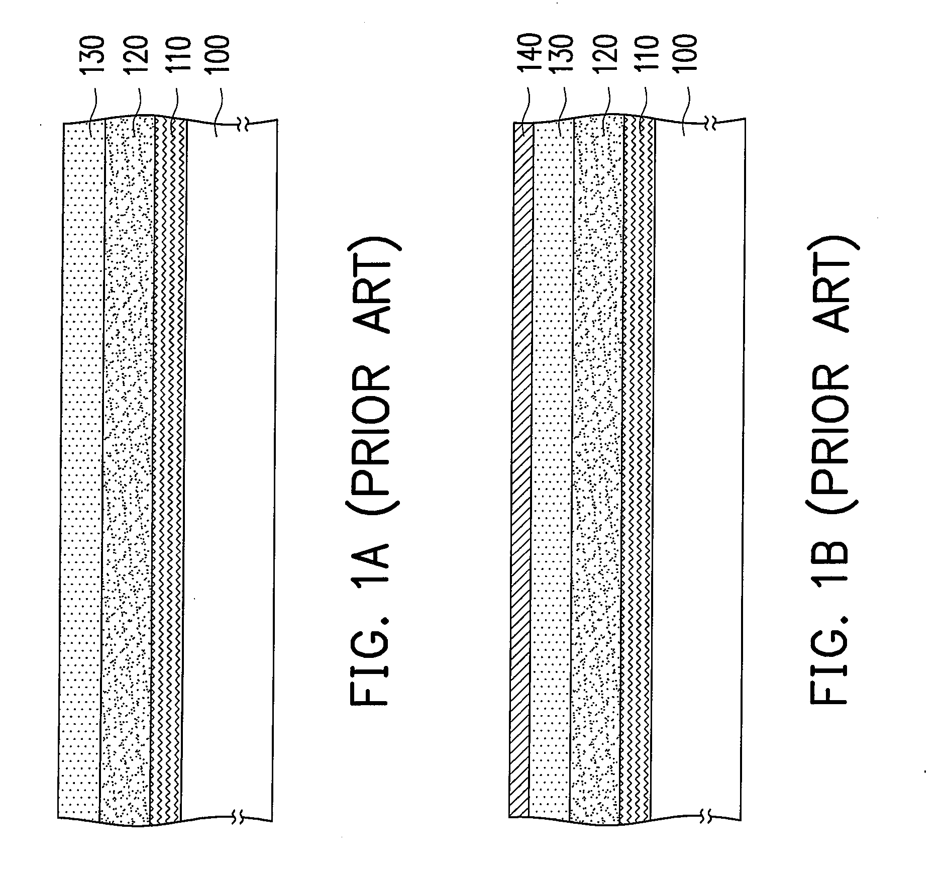
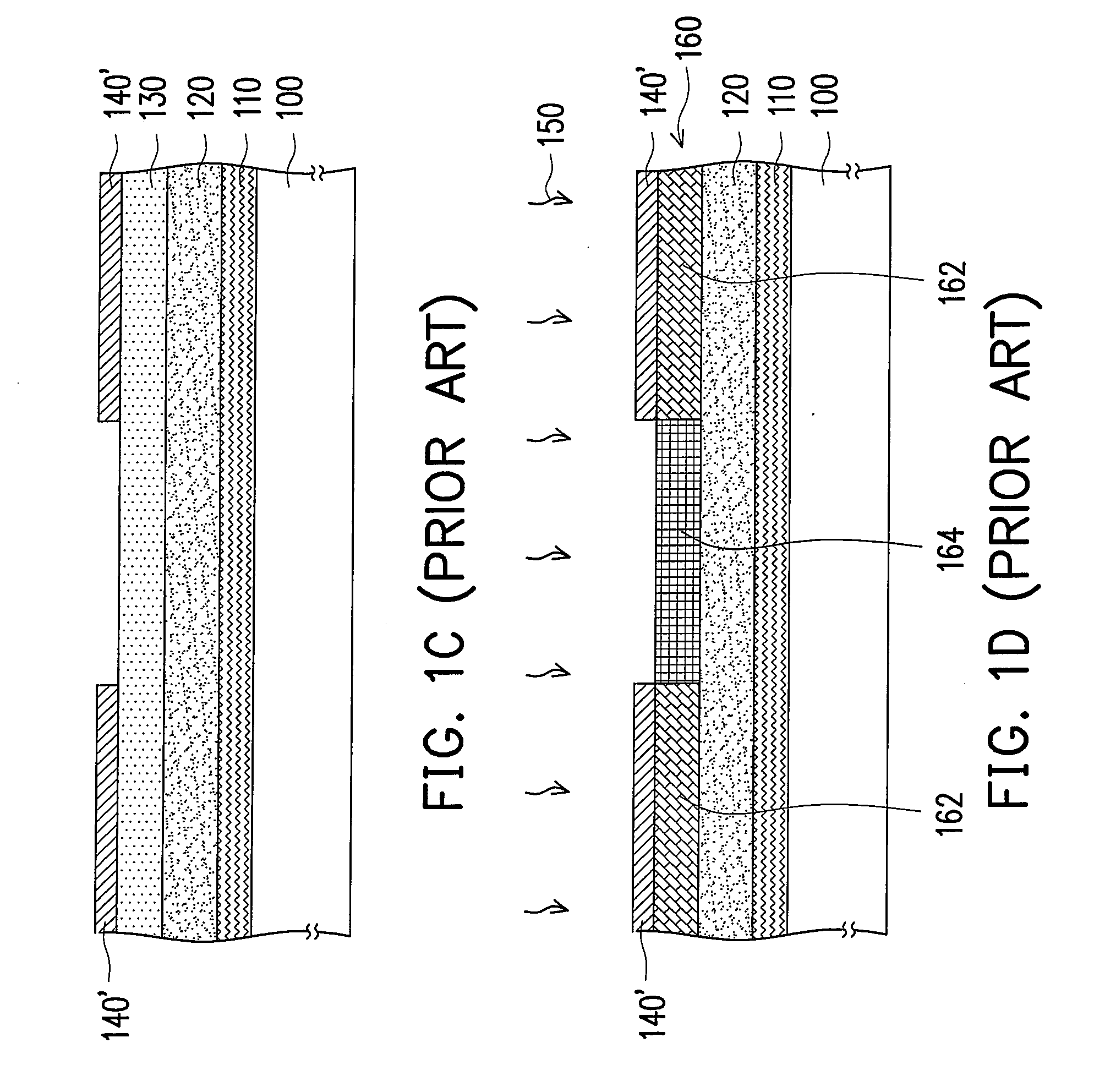
However, this method comes along with many problems, such as high power consumption, small grain size, much defects in the polysilicon layer, poor uniformity, and narrow process window etc.
Thereby, the conventional fabrication methods of polysilicon layer cannot be simplified and the fabrication cost thereof is high.

Method used


Image

  • Fabrication method of polysilicon layer
  • Fabrication method of polysilicon layer
  • Fabrication method of polysilicon layer

Examples


first embodiment

[0039]FIGS. 3A˜3E are cross-sectional views illustrating a fabrication method of a polysilicon layer according to the first embodiment of the present invention. First, referring to FIG. 3A, a substrate 300 is provided, wherein the substrate 300 may be a glass substrate or a silicon substrate.

[0040]Next, referring to FIG. 3A again, an amorphous silicon layer 330 is formed on the substrate 300. The amorphous silicon layer 330 may be formed through chemical vapour deposition (CVD). In an embodiment of the present invention, an adhesive layer 310 and a barrier layer 320 are further formed on the substrate 300 before the amorphous silicon layer 330 is formed on the substrate 300, wherein the adhesive layer 310 is disposed on the substrate 300, and the barrier layer 320 is disposed on the adhesive layer 310. The adhesive layer 310 and the barrier layer 320 may be formed through CVD. The material of the adhesive layer 310 may be silicon nitride, and the material of the barrier layer 320 ma...

second embodiment

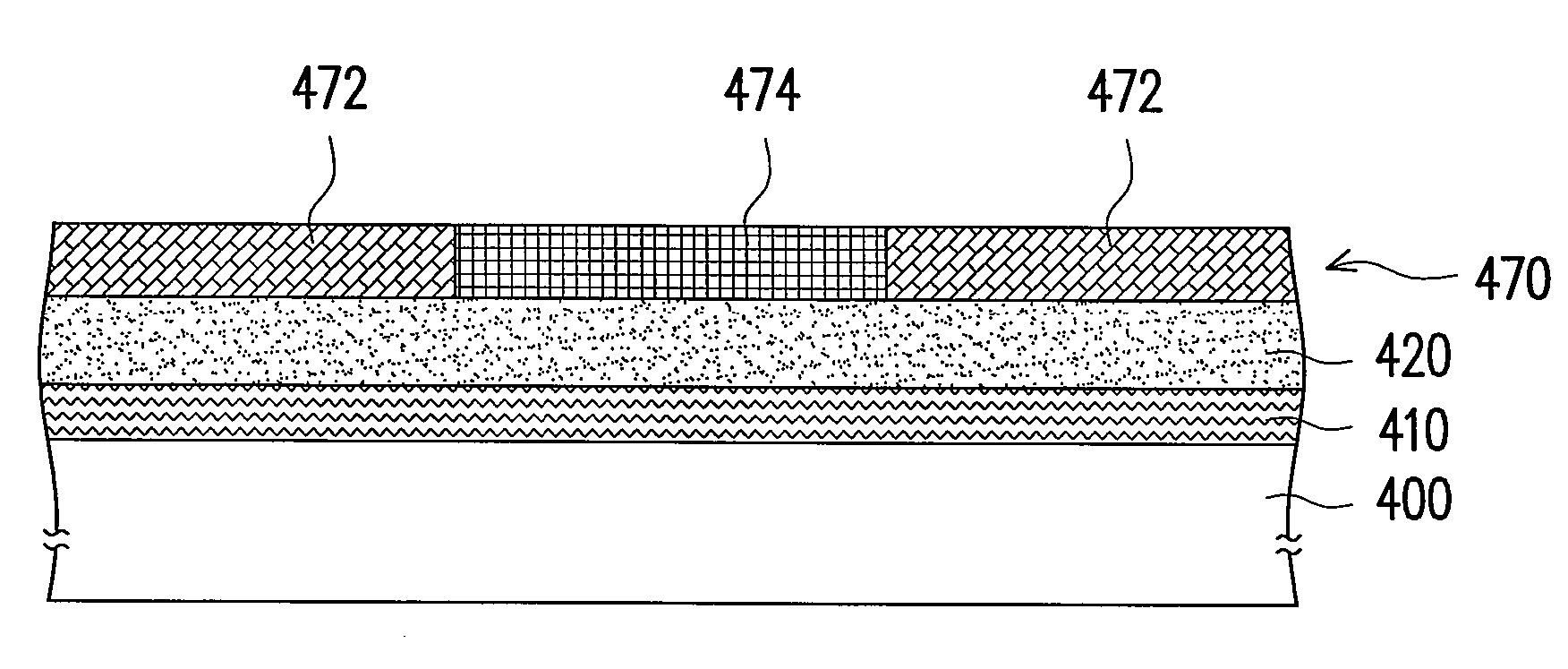
[0047]FIGS. 4A˜4E are cross-sectional views illustrating a fabrication method of a polysilicon layer according to the second embodiment of the present invention. First, referring to FIG. 4A, a substrate 400 is provided, wherein the substrate 400 may be a glass substrate or a silicon substrate.

[0048]Next, referring to FIG. 4A again, an amorphous silicon layer 430 is formed on the substrate 400. The amorphous silicon layer 430 may be formed through CVD. In an embodiment of the present invention, an adhesive layer 410 and a barrier layer 420 are further formed on the substrate 400 before the amorphous silicon layer 430 is formed on the substrate 400, wherein the adhesive layer 410 is disposed on the substrate 400, and the barrier layer 420 is disposed on the adhesive layer 410. The adhesive layer 410 and the barrier layer 420 may be formed through CVD. The material of the adhesive layer 410 may be silicon nitride, and the material of the barrier layer 420 may be silicon oxide. The func...


PUM


Abstract

A fabrication method of a polysilicon layer is provided. First, a substrate is provided. Then, an amorphous silicon layer is formed on the substrate. After that, a patterned photomask having a light transmitting area and a light shielding area is provided, and the amorphous silicon layer is irradiated with a light by using the patterned photomask as a mask, wherein the amorphous silicon layer corresponding to the light transmitting area is transformed into a hydrophilic amorphous silicon layer, and the amorphous silicon layer corresponding to the light shielding area remains as a hydrophobic amorphous silicon layer. Next, a hydrophilic metal catalyst is provided and disposed on the hydrophilic amorphous silicon layer. After that, an annealing process is performed to transform the hydrophilic metal catalyst into a metal catalyst layer, and the metal catalyst layer reacts with the amorphous silicon layer to form a polysilicon layer.

Description

CROSS-REFERENCE TO RELATED APPLICATION[0001]This application claims the priority benefit of Taiwan application serial no. 96135674, filed on Sep. 26, 2007. The entirety the above-mentioned patent application is hereby incorporated by reference herein and made a part of specification.BACKGROUND OF THE INVENTION[0002]1. Field of the Invention[0003]The present invention generally relates to a fabrication method of a semiconductor layer, in particular, to a fabrication method of a polysilicon layer.[0004]2. Description of Related Art[0005]Thin film transistor liquid crystal display (TFT-LCD) has become the mainstream in today's flat panel display market. TFT-LCD can be categorized into amorphous silicon TFT-LCD and low-temperature polysilicon (LTPS) TFT-LCD according to the material of the channel layer thereof.[0006]The electron mobility of an LTPS TFT is above 200 cm2 / V-sec so that the LTPS TFT can be fabricated in small size. Thus, high aperture ratio can be achieved by an LTPS TFT-L...

Claims


Application Information

Patent Timeline
IPC IPC(8): H01L21/20
CPCH01L21/0237H01L21/02488H01L27/1277H01L21/02672H01L21/02532
Inventor TSAI, YI-YUNCHIU, SHAO-YUMA, CHIA-HSUANYU, PEI-CHEN
Owner CHUNGHWA PICTURE TUBES LTD
Learn More