Printed circuit board with embedded chip capacitor and chip capacitor embedment method

a technology of embedded chips and printed circuit boards, which is applied in the direction of cross-talk/noise/interference reduction, sustainable manufacturing/processing, and final product manufacturing, etc., can solve the problems of obstructing the accurate operation of the rf circuit, difficult to accurately receive the signal having a certain frequency band, and difficulty in mixing signals, etc., to achieve simple structure, prevent noise, and high capacity

Inactive Publication Date: 2009-04-02
SAMSUNG ELECTRO MECHANICS CO LTD
View PDF10 Cites 17 Cited by
  • Summary
  • Abstract
  • Description
  • Claims
  • Application Information

AI Technical Summary

Benefits of technology

[0023]The present invention also provides a printed circuit board having an embedded chip capacitor that can simply prevent the noise having a desired frequency band by using the cavity capacitor having a simple structure as an electromagnetic bandgap structure.
[0024]In addition, the present invention provides a compact, thin film and light-weighted printed circuit board having an embedded chip capacitor with high capacity and high efficiency through a simple fabrication process and a reduced fabrication time and cost.

Problems solved by technology

This problem results in obstructing the accurate operation of the RF circuit 140.
For example, when the RF circuit 140 receives a signal having a certain frequency band, transferring the EM wave 150 including the signals having the certain frequency band from the digital circuit 130 may make it difficult to accurately receive the signal having the certain frequency band.
Solving the problem mixed signals becomes more difficult due to the higher operation frequency of the digital circuit 130 according to the increased complexity of electronic apparatuses.
The decoupling capacitor method, which is a typical solution for power noise, is not adequate for high frequencies.
However, the foregoing electromagnetic bandgap structure may not satisfy the two conditions needed to solve the mixed signal problem simultaneously.
However, this may have a bad influence on signal integrity.
Also, in the case of having the complex line structure in which the digital circuit and the RF circuit are realized on the same board like the main board of a mobile phone or mounting a lot of active elements and passive elements in the same small-sized board as a system in package (SiP) board, a lot of design limitations are required to be recovered to realize the electromagnetic bandgap structure by the conventional mushroom type structure.

Method used


Image

  • Printed circuit board with embedded chip capacitor and chip capacitor embedment method
  • Printed circuit board with embedded chip capacitor and chip capacitor embedment method
  • Printed circuit board with embedded chip capacitor and chip capacitor embedment method

Examples


first embodiment

[0073]FIG. 6 is a side view showing a printed circuit board having an embedded chip capacitor in accordance with the present invention, and FIG. 7 is a schematic view showing an equivalent circuit of the printed circuit board shown in FIG. 6.

[0074]Referring to FIG. 6, a printed circuit board having an embedded chip capacitor in accordance with a first embodiment of the present invention can include a first conductive layer 310, a second conductive layer 320, a dielectric layer 330, a chip capacitor 340 and a via 350.

[0075]Any one of the first conductive 310 and the second conductive layer 320 can be used as a power layer, and the other can be used as a ground layer. Accordingly, the first conductive 310 and the second conductive layer 320 can be away from each other through the dielectric layer 330 placed therebetween in order to allow the first conductive 310 and to be electrically disconnected to the second conductive layer 320.

[0076]The chip capacitor 340 can be embedded between ...

third embodiment

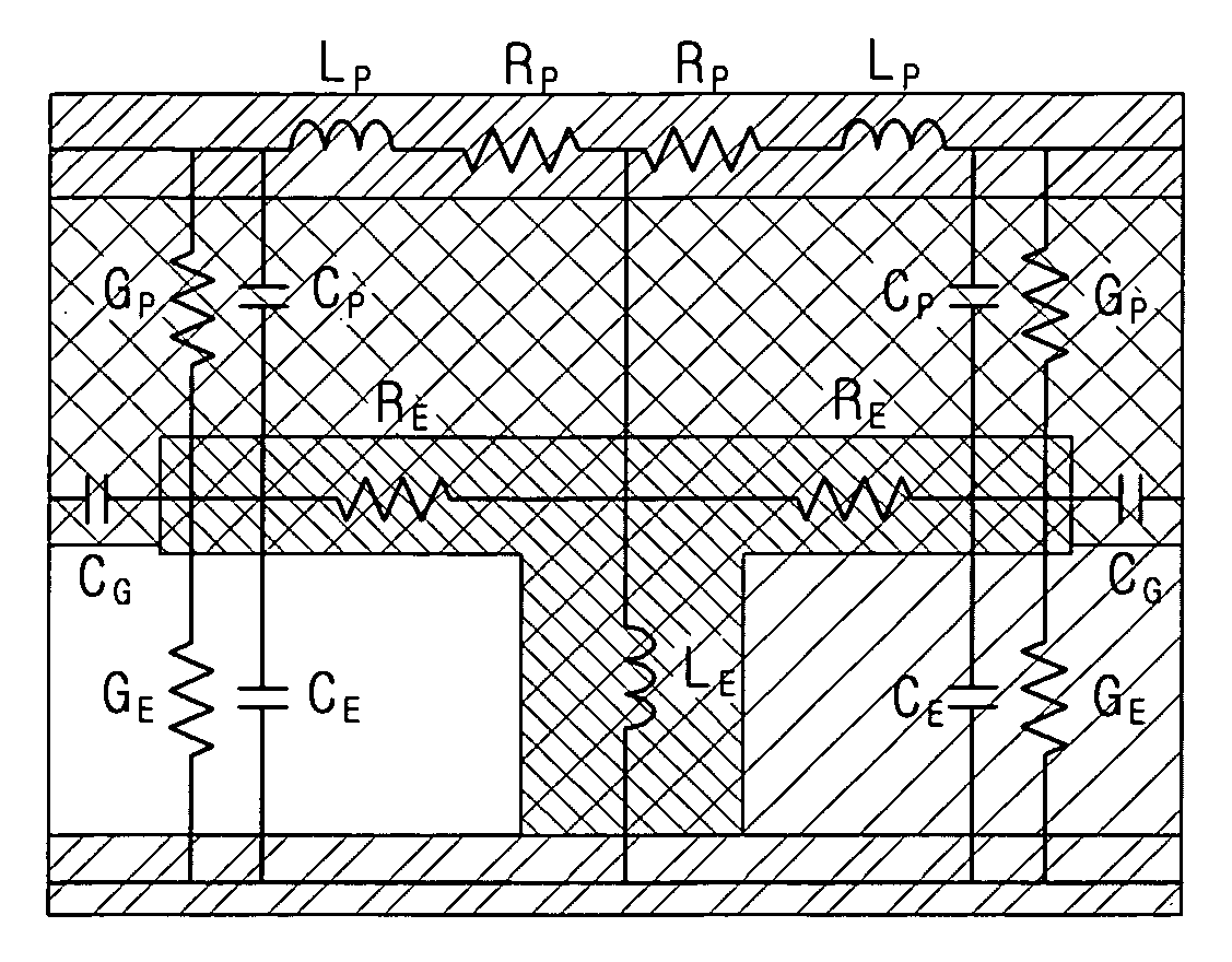
[0084]Accordingly, the printed circuit board in accordance with the second or third embodiment of the presented invention can more efficiently and universally use the function as the electromagnetic bandgap structure intercepting the transfer of an electromagnetic wave having a desired frequency band by the etched pattern 370, which is additionally connected to the chip capacitor 340 in series, together with the inductance component by the via 350 (refer to FIG. 8C and FIG. 9C). This is because adjusting the inductance value according to the design modification of the diameter, length and shape of the via 350 between any two conductive layers of the printed circuit board having the determined size, thickness and area size can not but be partially restricted.

[0085]As compared with this, to obtain a desired inductance value by designing and controlling the shape, length, width and area size of the etched pattern 370 can be more easily performed on the design. This can increase the usa...

fourth embodiment

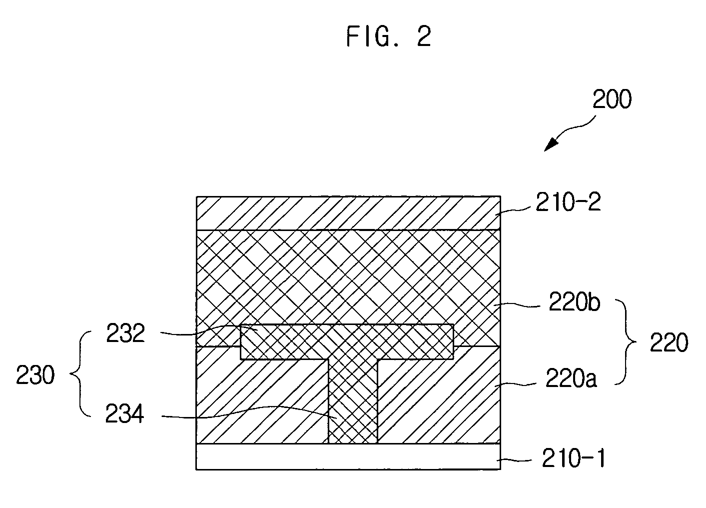
[0087]FIG. 10A is a side view showing a printed circuit board having an embedded chip capacitor in accordance with the present invention, and FIG. 10B illustrates a clearance hole when the printed circuit board shown in FIG. 10A is viewed from an upper side.

[0088]Referring to FIG. 10A and FIG. 10B, a printed circuit board having an embedded chip capacitor in accordance with a fourth embodiment of the present invention can have the shape in which a clearance hole 360 is formed in a part of the second conductive layer 320.

[0089]The reason that the clearance hole 360 is formed at the second conductive layer 320 in the printed circuit board in accordance with the fourth embodiment of the present invention is as follows. All chip capacitors embedded in the printed circuit board in accordance with the forgoing embodiments are the flake type. The flake type indicates that the electrodes are formed in an upper side and a lower side, respectively, and the dielectric member is placed between ...


PUM

PropertyMeasurementUnit
frequencyaaaaaaaaaa
frequencyaaaaaaaaaa
dielectric constantaaaaaaaaaa

Abstract

A printed circuit board having an embedded chip capacitor is disclosed. According to an embodiment of the present invention, a printed circuit board having an embedded chip capacitor can include a first conductive layer; a second conductive layer, placed away from the first conductive layer; a chip capacitor, placed between the first conductive layer and the second conductive layer and having a second electrode, connected to the second conductive layer; and a via, connecting the first conductive layer to a first electrode of the chip capacitor. With the present invention, a problem mixed signals can be solved in the printed circuit board including an analog circuit and a digital circuit board by using the chip capacitor embedded in the printed circuit board as an electromagnetic bandgap structure. Here, various electrical devices or elements are mounted in the printed circuit board.

Description

CROSS-REFERENCE TO RELATED PATENT APPLICATIONS[0001]This application claims the benefit of Korean Patent Application No. 10-2007-0097722, filed on Sep. 28, 2007, in the Korean Intellectual Property Office, the disclosure of which is incorporated herein in its entirety by referenceBACKGROUND OF THE INVENTION[0002]1. Field of the Invention[0003]The present invention relates to a printed circuit board, more specifically to a printed circuit board having an embedded chip capacitor and a chip capacitor embedding method that can use a series connection structure between a chip capacitor and a via as an electromagnetic bandgap structure.[0004]2. Background Art[0005]Various apparatuses such as mobile communication terminals, personal digital assistants (PDA), laptop computers and digital multimedia broadcasting (DMB) devices have been launched in order to meet today's trend that mobility is considered as one of the most important issues.[0006]Such apparatuses include a printed circuit board...

Claims


Application Information

Patent Timeline
Patent Type & Authority Applications(United States)
IPC IPC(8): H03H7/00H05K3/30
CPCH01L2224/16225H05K1/0231H05K1/0236H05K1/165H05K1/185H05K2201/093Y10T29/4913H05K2201/09509H05K2201/09663H05K2201/10636H05K2201/10643Y10T29/49146H05K2201/09309Y02P70/50H05K1/16
Inventor KIM, HANYOO, JE-GWANGHAN, MI-JAPARK, DAE-HYUN
Owner SAMSUNG ELECTRO MECHANICS CO LTD
Why Eureka
Try Eureka