Printed circuit board coil

a printed circuit board and coil technology, applied in the field of electromagnetic coils, can solve the problems of increasing the overall cost of the sheath, affecting the effect of the printed circuit, so as to reduce the skin effect, reduce the loss, and simple and effective

Active Publication Date: 2009-04-02
PHILIPS IP VENTURES BV
View PDF13 Cites 497 Cited by
  • Summary
  • Abstract
  • Description
  • Claims
  • Application Information

AI Technical Summary

Benefits of technology

[0009]The present invention provides a simple and effective PCB coil that overcomes important disadvantages of prior PCB coils, while maintaining many of the advantages of PCB coils. The presence of multiple, undulating current flow paths reduces skin effect and lower losses compared to conventional PCB coils. The use of segmentation and interlayer connectors provides a reliable and easily implemented structure for electrically coupling the coil in the desired undulating pattern. Additionally, the undulation pattern of the filaments provides a coil in which each filament spends a substantially equal amount of time in proximity to the paired coil, which further improves efficiency of the coil because each filament contributes substantially equally to the self or mutual inductance of the coil. The present invention can also be implemented with inward / outward undulations to further simulate the current flow path of the strands of litz wire coils. The use of segmentation and interlayer connectors can lower parasitic capacitance by 1) decreasing the coil surface area to the segment surface area; and 2) introducing fringe effects that cancel each other out. Less capacitance allows inductance in the coil to be maximized which can result in lower resistance and less losses. These benefits are all provided while in a PCB coil that has thinner coils and allows for tighter coupling than a bulkier litz wire coil.

Problems solved by technology

Second, the resulting structure is relatively delicate and each strand is subject to breakage.
This sheath adds to the overall cost and provides even more resistance over that theoretically achievable.
Fourth, the manufacturing process for litz wire and litz wire coils is relatively expensive and requires special, costly equipment.
Fifth, the litz wire may be bulkier than desired for some applications because of packing density from wire to wire and the space occupied by the insulation between strands.
Wire coils are relatively expensive to manufacture (particularly litz wire coils), occupy a relatively large amount of space and often require mechanical mounting of the coil to a printed circuit board.
Although printed circuit board coils can present some advantages over wire coils, conventional printed circuit board coils suffer from certain problems faced by conventional solid wires, such as those associated with uneven distribution of induced current and uneven distribution of inductance within the PCB coil.
Further, stacked PCB coils can introduce unwanted parasitic capacitance due to some of the coils receiving more of the magnetic field than others.
Ultimately, this can result in higher resistance and losses.

Method used


Image

  • Printed circuit board coil
  • Printed circuit board coil
  • Printed circuit board coil

Examples


Embodiment Construction

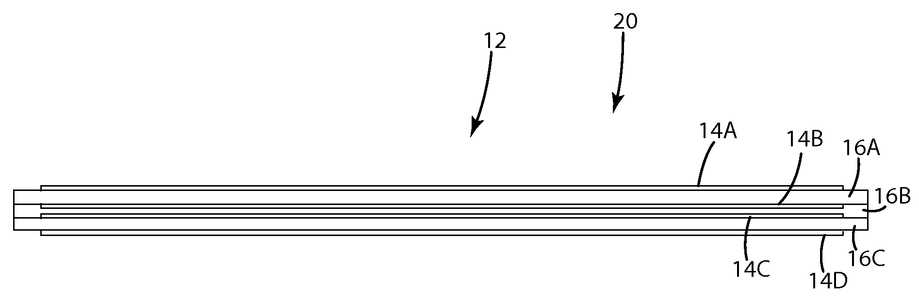
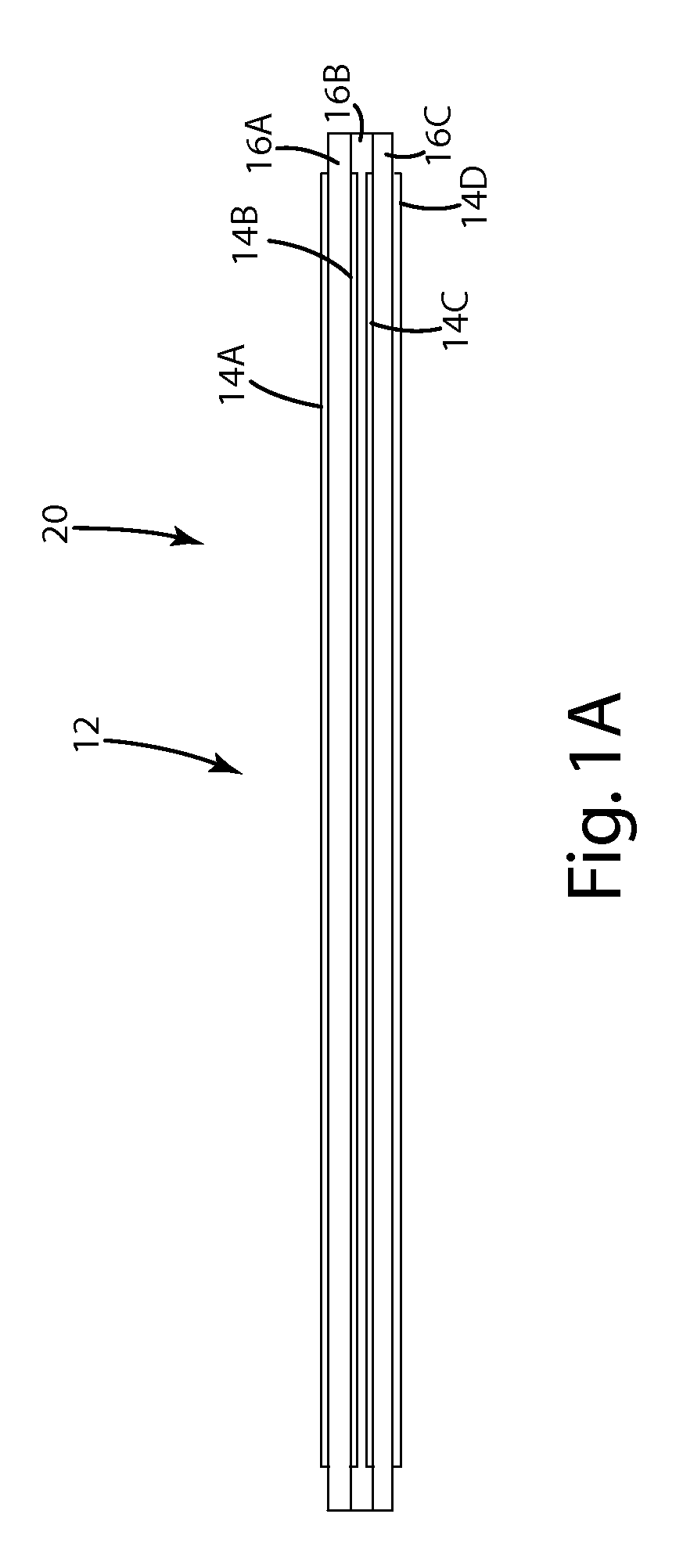
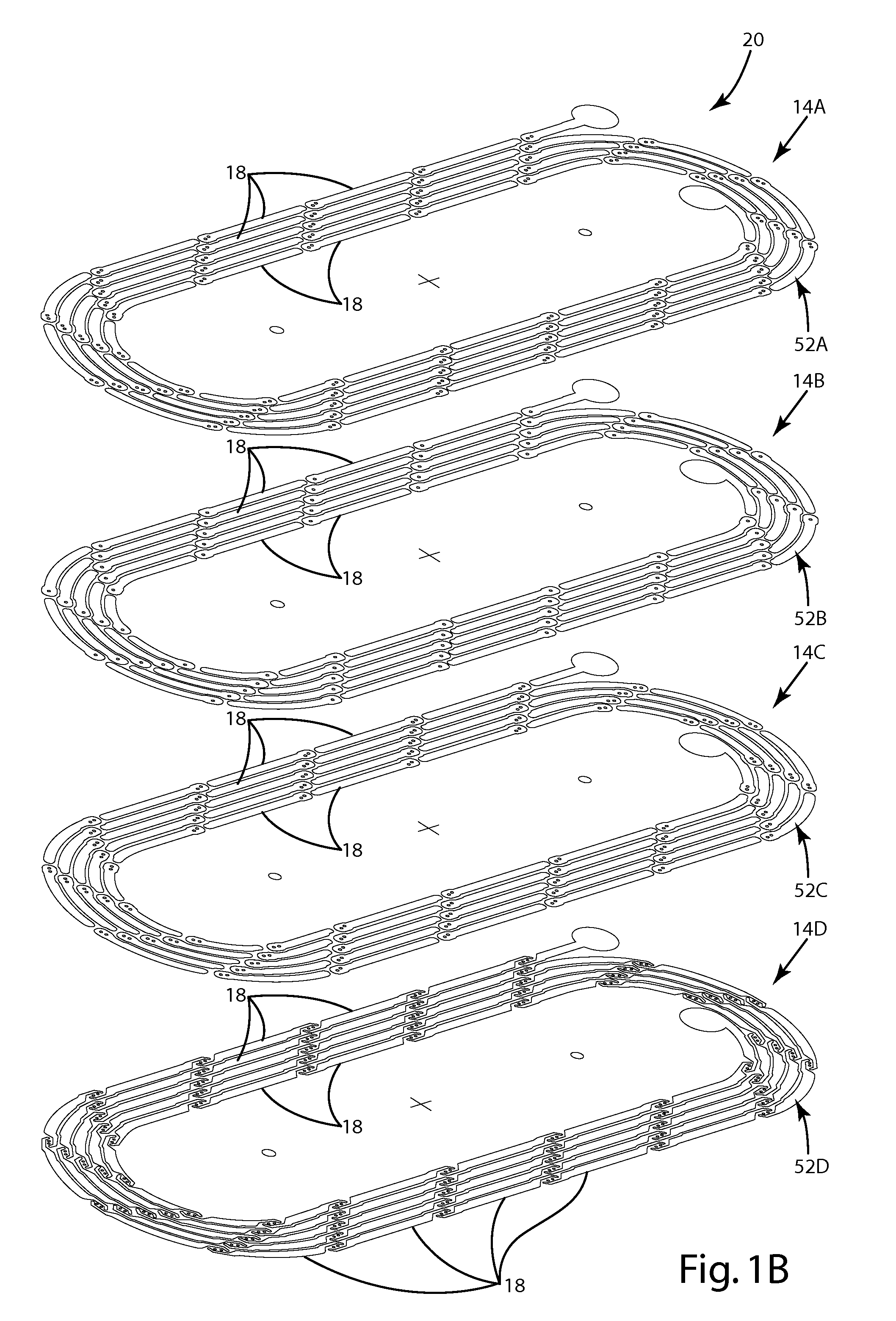
[0040]A printed circuit board (“PCB”) coil 20 in accordance with an embodiment of the present invention is shown in FIGS. 1A, 1B and 1C. The PCB coil 20 generally includes a plurality of alternating conductor layers 14a-d and insulator layers 16a-c that cooperatively form a multilayer coil (See FIG. 1A). Each conductor layer 14a-d includes a trace 52a-d defined by a plurality of discrete segments 18 (See FIG. 1B). The segments 18 of different traces 52a-d in different conductor layers 14a-d are interconnected by connectors 40 to define “filaments”54a-d (discrete current flow paths) that undulate through the layers in a predetermined pattern (See FIGS. 1C, 6 and 7). The predetermined pattern is designed so that there will be a substantially even distribution of power induced among the filaments 54a-d when the PCB coil is paired with a second inductive coil. In the illustrated embodiment, the PCB coil 20 simulates a litz wire coil in that the filaments 54a-d, though offset, follow sub...


PUM

PropertyMeasurementUnit
timeaaaaaaaaaa
inductanceaaaaaaaaaa
magnetic fluxaaaaaaaaaa

Abstract

A multilayer printed circuit board (“PCB”) coil that simulates a coil formed from litz wire. The PCB includes a plurality of alternating conductor and insulating layers interconnected to cooperatively form the coil. Each conductor layer includes a trace that follows the desired coil shape and is divided into a plurality of discrete conductor segments. The segments are electrically connected across layers to provide a plurality of current flow paths (or filaments) that undulate between the layers in a regular, repeating pattern. The coil may be configured so that each filament spends a substantially equal amount of time in proximity to the paired coil and therefore contributes substantially equally to the self or mutual inductance of the coil. Each conductor layer may include a plurality of associated traces and intralayer connector that interconnected so that each filament undulates not only upwardly/downwardly, but also inwardly/outwardly in a regular, repeating pattern.

Description

BACKGROUND OF THE INVENTION[0001]The present invention relates to electromagnetic coils, and more particularly to multilayer printed circuit board electromagnetic coils.[0002]Electromagnetic coils are used in a wide variety of electrical applications in connection with the inductive transfer of power. For example, different forms of electrical coils are used in transformers, inductive power couplings and motors. Historically, electrical coils have been formed by wrapping a strand of wire into one or more loops. Typically, the diameter of the coil, the type and diameter of the wire, the number of loops (or turns) and other characteristics of the wire and the coil are selected to provide the desired electromagnetic power transfer characteristics.[0003]It is well known that alternating electrical current (AC) has a tendency to distribute itself within a conductor so that the current density near the surface of the conductor is greater than at its core. This phenomenon is commonly refer...

Claims


Application Information

Patent Timeline
Patent Type & Authority Applications(United States)
IPC IPC(8): H01F5/00
CPCH01F5/003H05K2201/097H05K1/165H05K1/0228H01F27/2804H01F27/34H01F38/14H01F2027/2809
Inventor BAARMAN, DAVID W.SCHWANNECKE, JOSHUA K.GUTHRIE, WARREN E.WAHL, RICHARD A.DUCKWORTH, PAUL
Owner PHILIPS IP VENTURES BV
Why Eureka
Try Eureka