Planar lightwave circuits with air filled trenches

a technology of lightwave circuits and air filled trenches, applied in nanotechnology, instruments, nanotechnology, etc., can solve problems such as air filled trenches, and achieve the effect of easy integration of photonic and electronic components

Inactive Publication Date: 2009-04-02
DOAN MY THE
View PDF6 Cites 82 Cited by
  • Summary
  • Abstract
  • Description
  • Claims
  • Application Information

AI Technical Summary

Benefits of technology

[0013]A principle object of the present invention is to provide an effective and very manufacturable method to integrate photonic and electronic components easier.

Problems solved by technology

Reducing the optical loss due to evanescent coupling to the substrate is achieved by removing the silicon under the waveguides and their cladding, resulting in air filled trenches.

Method used


Image

  • Planar lightwave circuits with air filled trenches
  • Planar lightwave circuits with air filled trenches
  • Planar lightwave circuits with air filled trenches

Examples


Embodiment Construction

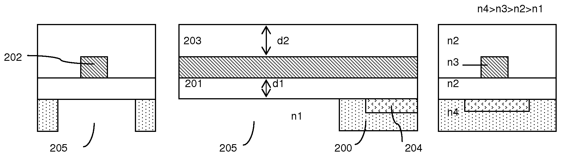
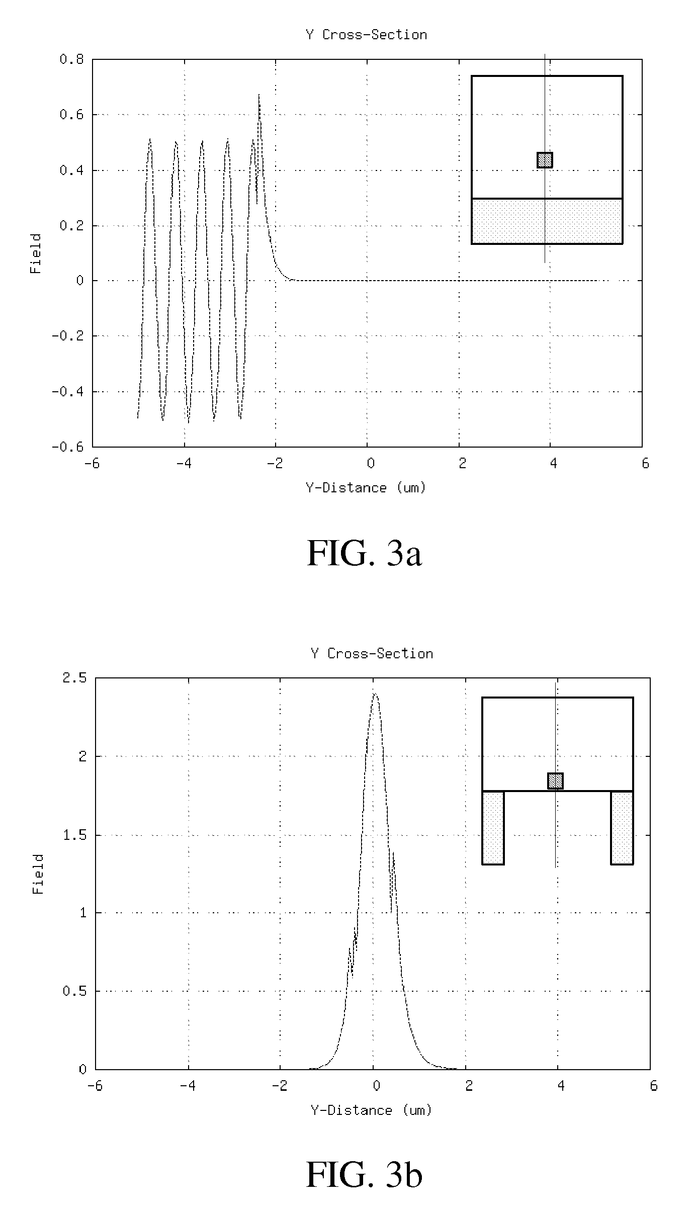
[0033]The preferred embodiments of the present invention disclose methods to reduce optical propagation loss, as well as, making it simpler to integrate waveguides to other on-chip functions, and to electronic circuits. On-chip functions can be photodetectors, tuning devices, modulator devices, dispersion compensation devices, etc. An embodiment of the present invention relates to the methods to reduce propagation loss due to evanescent coupling to the substrate by selectively etching away the substrate under the waveguides, thus leaving air filled trenches. Examples of how the preferred embodiments can improve the coupling efficient to the photodetectors, can improve the performances of waveguides to on-chip devices that utilized semiconductor-on-insulator substrate, can reduce losses in both photonic and electronic circuits, and can improve the sensitivity of an optical sensor will be highlighted.

[0034]It should be clear to those experienced in the art that the present invention c...


PUM


Abstract

An air filled trench is formed underneath the waveguide to reduce propagation loss, which in turn allowing the waveguide to be in the close proximity of on-chip devices, such as a photodetector. The air filled trench is formed from the back side of the substrate; hence it would not disturb the integration and the formation of components on the front side of the substrate. In another embodiment, for silicon-on-insulator (SOI) based device, with an air filled trench and a metal electrode, a back gate is formed. In yet another embodiment, air filled trench also reduces the substrate loss of RF passive components and passive antenna operating in Giga Hertz range. Air filled trenches can be used for both photonic and electronic circuits in a planar lightwave circuit. Finally, another embodiment is for the trench to effectively guide gases and fluids to pass through the detection area.

Description

BACKGROUND OF THE INVENTION[0001](1) Field of the Invention[0002]The invention relates to the formation of low loss planar lightwave circuit, more particularly to the use of air filled trench to reduce loss due to the substrate and to make the integration of waveguide to on-chip device easier.[0003](2) Background[0004]There are various methods to integrate optical components and electronics for networking, sensing and displays. The current and popular method is the hybrid integration of various components such as laser diodes, photodetectors, waveguides and VLSI chips on a silicon optical bench, as described in Kitigawa et al., “Hybrid Integration Technologies using planar lightwave circuits and developed components,” IEICE Trans. Electron, Vol. E85-C, No. 4, April 2002, p. 1009. Each of the components are picked, aligned, placed and bonded onto a silicon substrate using flip chip technology. The performance of such module is sensitive to the alignments among the optical components ...

Claims


Application Information

Patent Timeline
Patent Type & Authority Applications(United States)
IPC IPC(8): G02B6/12
CPCB82Y20/00G01N21/7703G01N2021/7789G02B6/125G02B6/1225G02B6/1226G02B6/12G01N21/7746
Inventor DOAN, MY THE
Owner DOAN MY THE
Why Eureka
Try Eureka