METHOD FOR FORMING RUTHENIUM COMPLEX FILM USING Beta-DIKETONE-COORDINATED RUTHENIUM PRECURSOR

a technology of ruthenium complex and precursor, which is applied in the direction of coatings, layered products, chemistry apparatus and processes, etc., can solve the problems of present problems and partially exposed barrier films, and achieve the effect of reducing the resistivity of the obtained ruthenium film

Inactive Publication Date: 2009-04-02
ASM JAPAN
View PDF99 Cites 49 Cited by
  • Summary
  • Abstract
  • Description
  • Claims
  • Application Information

AI Technical Summary

Benefits of technology

[0012]Here, X1 and X2 are hydrocarbons that are independent of each other or for each ligand, where X1 and X2 may form a hydrocarbon ring. Both X1 and X2 are desirably an alkyl group (such as an alkyl group having 1 to 4 carbon atoms), expressed by CR1R2R3 in an embodiment, where R1, R2 and R3 are hydrogen or CmH2 m+1 (m=1 to 3) (preferably a hydrogen or ethyl group) and independent of one another. Also, n is a value between 1 and 4, or 2 or 3 in an embodiment. Each β-diketone coordinat

Problems solved by technology

In reality, however, a laminated structure constituted by a copper diffusion barrier film and Ru film prevents the formation of continuous film when the Ru film is made t

Method used


Image

  • METHOD FOR FORMING RUTHENIUM COMPLEX FILM USING Beta-DIKETONE-COORDINATED RUTHENIUM PRECURSOR
  • METHOD FOR FORMING RUTHENIUM COMPLEX FILM USING Beta-DIKETONE-COORDINATED RUTHENIUM PRECURSOR
  • METHOD FOR FORMING RUTHENIUM COMPLEX FILM USING Beta-DIKETONE-COORDINATED RUTHENIUM PRECURSOR

Examples


example 1

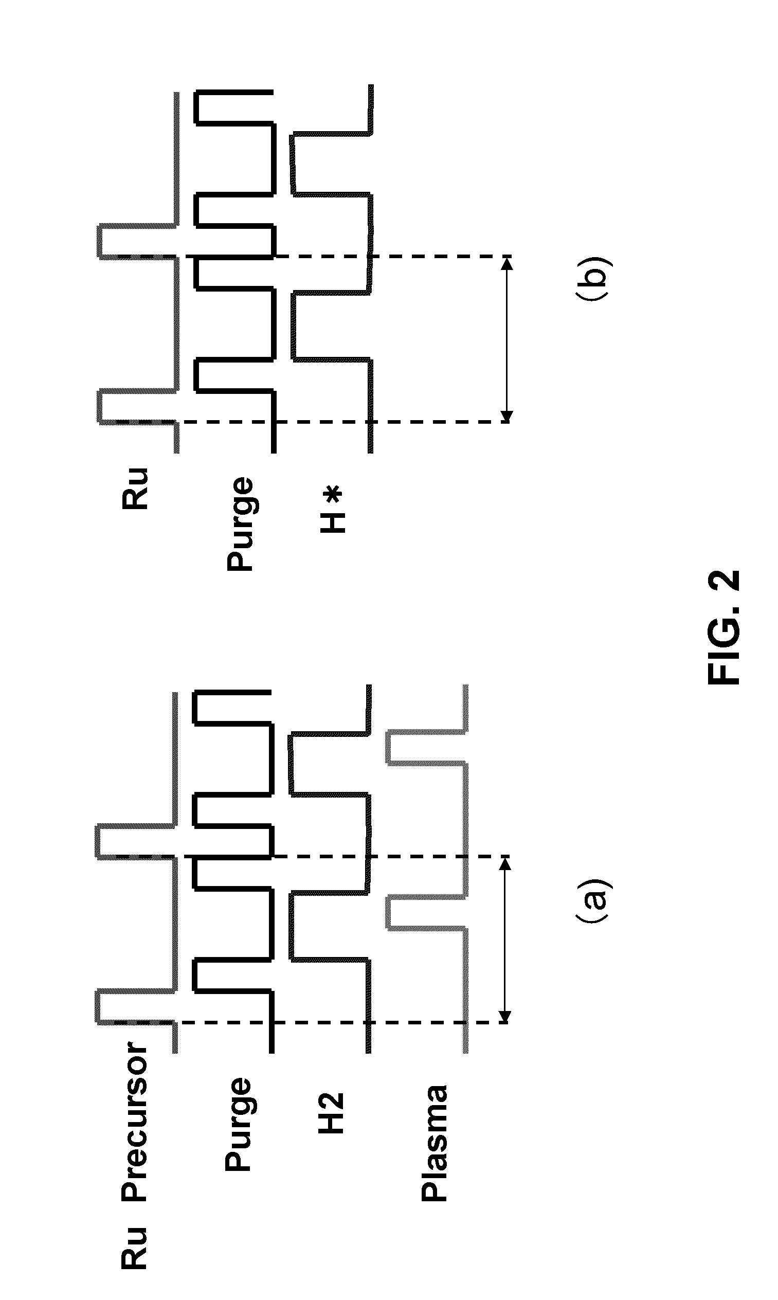
[0164]Application of a Ru film to semiconductor copper wiring using the process sequence shown in FIG. 2(a) is explained by using the schematic cross-section structure view in FIG. 3.

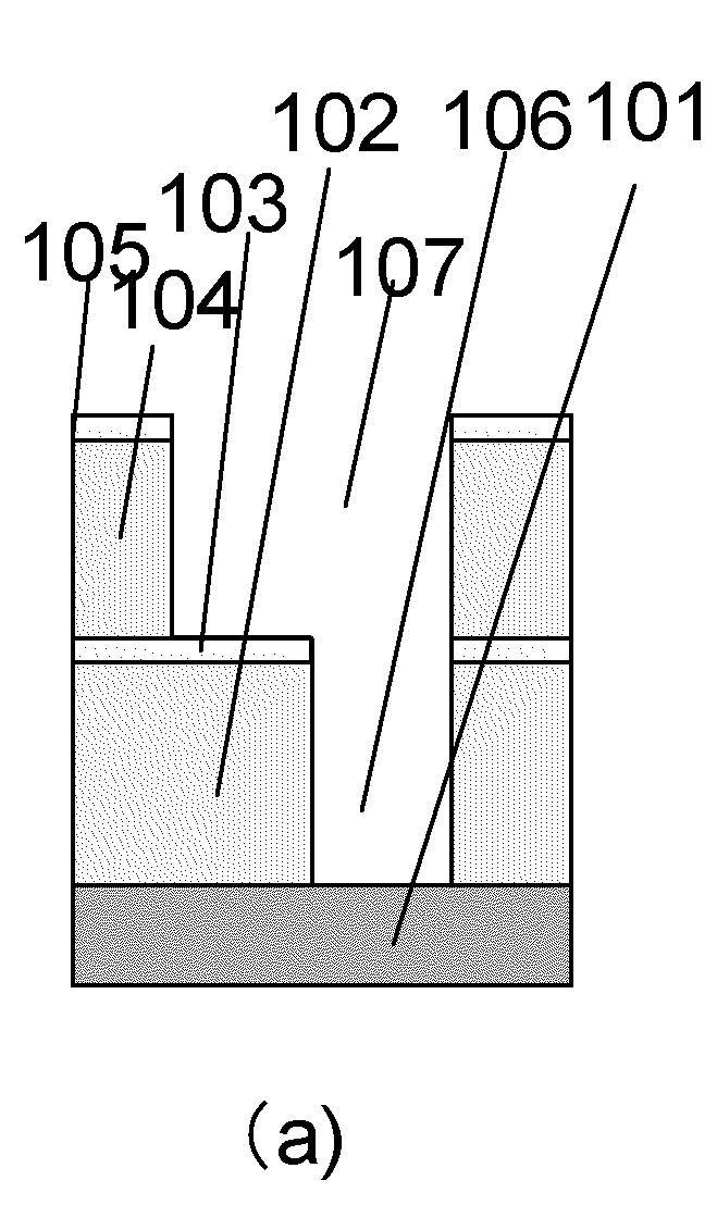
[0165]FIGS. 4(a) to (f) show a process for forming a Cu wiring by forming a Cu barrier film via dual damascene wiring and then forming a Cu seed layer, followed by Cu plating and Cu CMP. In FIG. 4(a), a via hole 106 is formed in an inter-layer insulation film 102 and a Cu barrier insulation film 103, and also a wiring trench 107 is formed in an inter-layer insulation film 104 and a Cu barrier insulation film 105, where all of the films are formed on a Cu lower-layer wiring 101. These via hole 106 and wiring trench 107 together constitute a Cu embedding range for dual damascene. In FIG. 4(b), a TaNxCy film 108 is formed over this range for 50 cycles, or approx. 3 nm, using the atomic layer deposition method using TIMATA (Tertiaryamylimidotris(dimethylamido)tantalum) material and hydrogen plasma. This for...

example 2

[0171]Application of a Ru film to capacitor electrodes of a dynamic random access memory, among various semiconductor memory devices, is explained using the schematic cross-section structure views of capacitor electrodes shown in FIGS. 10(a) to (c).

[0172]FIG. 10(a) shows the condition before the lower-layer electrode of a memory capacity is formed in the manufacturing process for dynamic random access memory cells having laminated capacitor electrodes. A silicon substrate 212 is in a so-called active range, being surrounded by an element separation range 213. Numeral 214 indicates a diffusion layer, and a conductive contact plug 216 is formed on the diffusion layer. Numeral 217 indicates a gate electrode, while numeral 219 indicates a conductive wire that becomes a bit wire. Numeral 218 is an inter-layer insulation film, numeral 221 is formed by the insulation film, and numeral 222 is a hole opening provided in a manner allowing a capacitor to be formed. A conductive layer connectin...

example 3

[0175]Application of a Ru film to semiconductor copper wiring using the process sequence in FIG. 2(a) is explained using the schematic cross-section structure view shown in FIG. 3.

[0176]FIGS. 11(a) to (f) show a process for forming a Cu wiring by forming a Cu barrier film via dual damascene wiring and then forming a Cu seed layer, followed by Cu plating and Cu CMP. In FIG. 11(a), a via hole 106 is formed in an inter-layer insulation film 102 and a Cu barrier insulation film 103, and also a wiring trench 107 is formed in an inter-layer insulation film 104 and a Cu barrier insulation film 105, where all of the films are formed on a Cu lower-layer wiring 101. These via hole 106 and wiring trench 107 together constitute a Cu embedding range for dual damascene. In FIG. 11(b), a Ru film 113 is formed for 25 cycles, or approx. 1 nm, using a Ru forming method conforming to an embodiment of the present invention. The sequence in FIG. 2(a) is used to supply a Ru material constituting a Ru pre...


PUM

PropertyMeasurementUnit
Thicknessaaaaaaaaaa
Thicknessaaaaaaaaaa
Nanoscale particle sizeaaaaaaaaaa

Abstract

A method for depositing a thin ruthenium (Ru) film on a substrate in a reaction chamber, comprising: step (i) of supplying at least one type of gas of a ruthenium precursor being a β-diketone-coordinated ruthenium complex and causing the gas to be adsorbed to the substrate in the reaction chamber; step (ii) of supplying a reducing gas into the reaction chamber and exciting the reducing gas, or supplying an excited reducing gas into the reaction chamber, in order to activate the ruthenium precursor adsorbed to the substrate; and step (iii) of repeating steps (i) and (ii) to form a thin ruthenium film on the substrate.

Description

CROSS-REFERENCE TO RELATED APPLICATIONS[0001]This application claims the benefit of U.S. Provisional Application No. 60 / 976,378, filed Sep. 28, 2007, and the disclosure of which is herein incorporated by reference in its entirety.BACKGROUND[0002]1. Field of the Invention[0003]The present invention relates to a method for forming a ruthenium (Ru) film for metal wiring structures that can be used favorably in the creation of fine semiconductor elements in general.[0004]2. Description of the Related Art[0005]Ru film is drawing the attention for its property to improve the adhesion with Cu, when a Ru film is formed at the interface between Cu and barrier metal in a Cu wiring structure which is the main wiring structure used in high-speed logic elements such as MPUs, and thereby significantly enhance the reliability of wiring. Methods are being studied to form a Ru film that provides a Cu diffusion barrier metal on a TaN film or WN film and then form a Cu film on top of the Ru film (one ...

Claims


Application Information

Patent Timeline
IPC IPC(8): B32B15/00C23C16/00
CPCC23C16/18C23C16/45542H01L21/76873H01L21/76843H01L21/76846H01L21/28562
Inventor SHINRIKI, HIROSHI
Owner ASM JAPAN
Why Eureka
Try Eureka