Light-emitting diode chip and manufacturing method thereof

a technology of light-emitting diodes and manufacturing methods, which is applied in the manufacturing of semiconductor/solid-state devices, semiconductor devices, electrical devices, etc., can solve the problems of high cost difficult heat dissipation, and complicated design and control of low-voltage high-current driving circuits. achieve the effect of high power load of large chips and high light-emitting efficiency

Inactive Publication Date: 2009-04-09
DELTA ELECTRONICS INC
View PDF8 Cites 16 Cited by
  • Summary
  • Abstract
  • Description
  • Claims
  • Application Information

AI Technical Summary

Benefits of technology

[0015]As mentioned hereinabove, the LED chip manufactured according to the above-mentioned method of the invention has a plurality of LED units connected in parallel or in series. The LED units with the smaller sizes are combined to form the LED chip with the larger size so that the high light emitting efficiency of the small chip and the high power load of the large chip can be provided.

Problems solved by technology

However, the design and the control of a low-voltage high-current driving circuit are more complicated than those of a high-voltage low-current driving circuit, and the low-voltage high-current driving circuit has the higher cost.
However, the heat dissipating is not so easy and the light emitting efficiency is deteriorated.
However, the complicated electrode pattern increases the difficulty in designing and manufacturing the LED and increases the cost of the LED.
In addition to the complicated electrode pattern, more than one gold wire has to be connected to one electrode in order to enhance the uniformity of the current so that the cost is increased and the manufacturing difficulty is increased.

Method used


Image

  • Light-emitting diode chip and manufacturing method thereof
  • Light-emitting diode chip and manufacturing method thereof
  • Light-emitting diode chip and manufacturing method thereof

Examples


first embodiment

[0028]Referring to FIG. 4, a manufacturing method of a LED chip according to a first embodiment of the invention includes steps S01 to S06. Illustrations will be made in the following with reference to FIGS. 5A to 5G.

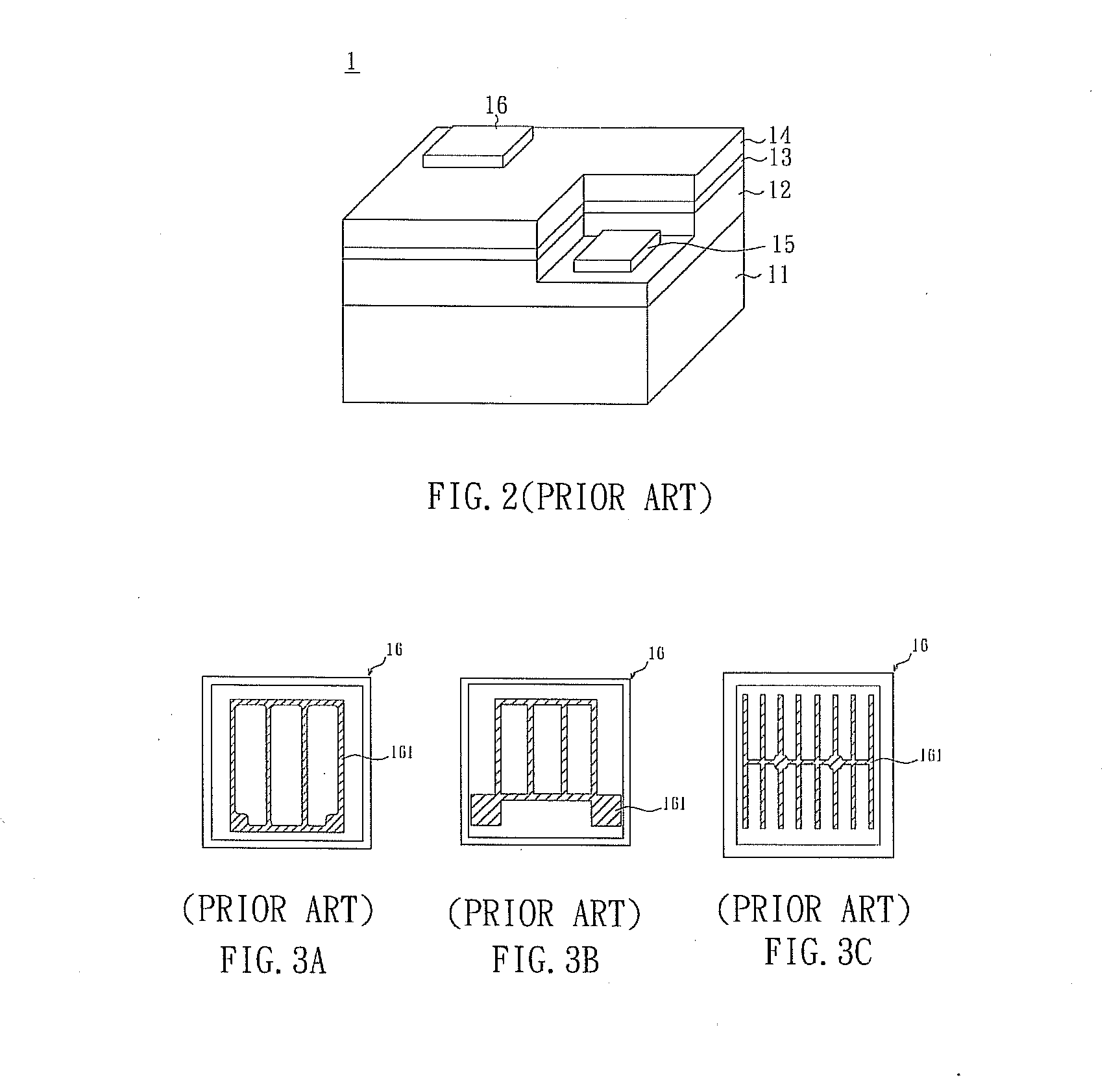
[0029]As shown in FIG. 5A, a buffer layer 22 is formed on a substrate 21 in the step S01. A material of the substrate 21 is, for example but not limited to, sapphire, silicon, silicon carbide or an alloy, and preferably has the high thermal conductivity. The buffer layer 22 is, for example but not limited to, a single layer substance or a multi-layer substance.

[0030]As shown in FIG. 5B, a first semiconductor layer 23, an active layer 24 and a second semiconductor layer 25 are formed in sequence in the step S02. The first semiconductor layer 23 can be formed on the buffer layer 22. Of course, the first semiconductor layer 23, the active layer 24 and the second semiconductor layer 25 can also be formed on an epitaxial substrate (not shown) in sequence, and then be transpo...

second embodiment

[0039]Referring to FIG. 7, a manufacturing method of a LED chip according to a second embodiment of the invention includes steps S11 to S17. Illustrations will be made with reference to FIGS. 8A to 8G.

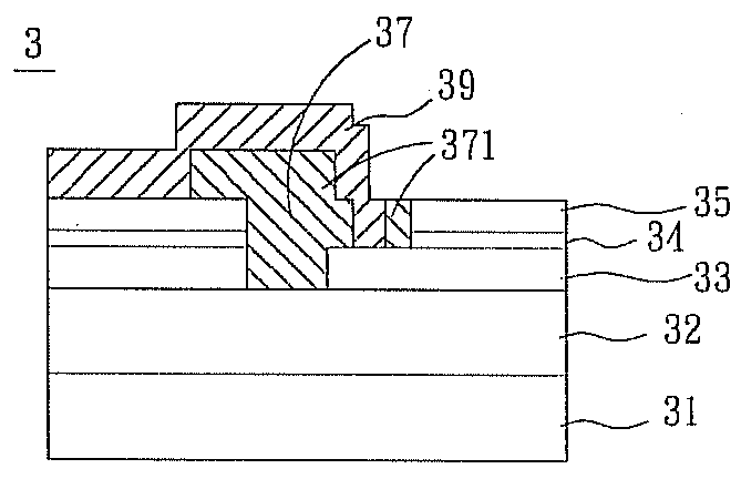
[0040]As shown in FIG. 8A, a buffer layer 32 is formed on a substrate 31 in the step S11. A material of the substrate 31 if, for example but not limited to, sapphire, silicon, silicon carbide or an alloy, and may preferably have the high thermal conductivity. The buffer layer 32 is, for example but not limited to, a single layer or a multi-layer.

[0041]As shown in FIG. 8B, a first semiconductor layer 33, an active layer 34 and a second semiconductor layer 35 are formed sequentially on the buffer layer 32 in sequence in the step S12. The first semiconductor layer 33 can be formed on the buffer layer 32. Of course, the first semiconductor layer 33, the active layer 34 and the second semiconductor layer 35 can also be formed on an epitaxial substrate (not shown) in sequence, and then be tr...


PUM


Abstract

A light-emitting diode (LED) chip includes a substrate, a first semiconductor layer, an active layer, a second semiconductor layer and a groove. The first semiconductor layer, active layer and second semiconductor layer are formed on the substrate in sequence. The groove is formed in the first semiconductor layer, the active layer and the second semiconductor layer.

Description

CROSS REFERENCE TO RELATED APPLICATIONS[0001]This Non-provisional application claims priority under 35 U.S.C. §119(a) on Patent Application No(s). 096137367 filed in Taiwan, Republic of China on Oct. 5, 2007, the entire contents of which are hereby incorporated by reference.BACKGROUND OF THE INVENTION[0002]1. Field of Invention[0003]The invention relates to a light-emitting diode (LED) chip and a manufacturing method thereof.[0004]2. Related Art[0005]A light-emitting diode (LED) apparatus is a lighting apparatus made of semiconductor materials. The LED apparatus pertaining to a cold lighting apparatus has the advantages of low power consumption, long lifetime, high response speed and small size, and can be manufactured into an extremely small or array-type apparatus. With the continuous progress of the recent technology, the application range thereof covers an indicator of a computer or a house appliance product, a backlight source of a liquid crystal display (LCD) apparatus, a traf...

Claims


Application Information

Patent Timeline
Patent Type & Authority Applications(United States)
IPC IPC(8): H01L33/00H01L21/00H01L33/08H01L33/12H01L33/20H01L33/28H01L33/32H01L33/38
CPCH01L27/156
Inventor TU, SHENG-HANSHEU, GWO-JIUNCHANG, CHII-HOWLIN, KUN-YUEH
Owner DELTA ELECTRONICS INC
Why Eureka
Try Eureka