Asymmetric-ldd mos device

a technology of mos and transistors, applied in the field ofmos devices, can solve the problems of reducing the maximum output power and efficiency of mos devices, restricting the use of cmos power amplifiers, and long rf soc design, which includes rf power amplifiers, and achieves low breakdown voltage problems. , the effect of improving the rf power performan

Inactive Publication Date: 2009-04-09
KING MINGCHU +1
View PDF3 Cites 15 Cited by
  • Summary
  • Abstract
  • Description
  • Claims
  • Application Information

AI Technical Summary

Benefits of technology

[0003]An objective of the present invention is to overcome the l

Problems solved by technology

However, the low drain breakdown voltage of CMOS transistors restricts the use of CMOS for power amplifiers.
This limitation for high voltage operation significantly reduces the maximum output power and efficiency for CMOS devices.
Therefore, the RF SoC desig

Method used


Image

  • Asymmetric-ldd mos device
  • Asymmetric-ldd mos device
  • Asymmetric-ldd mos device

Examples


Embodiment Construction

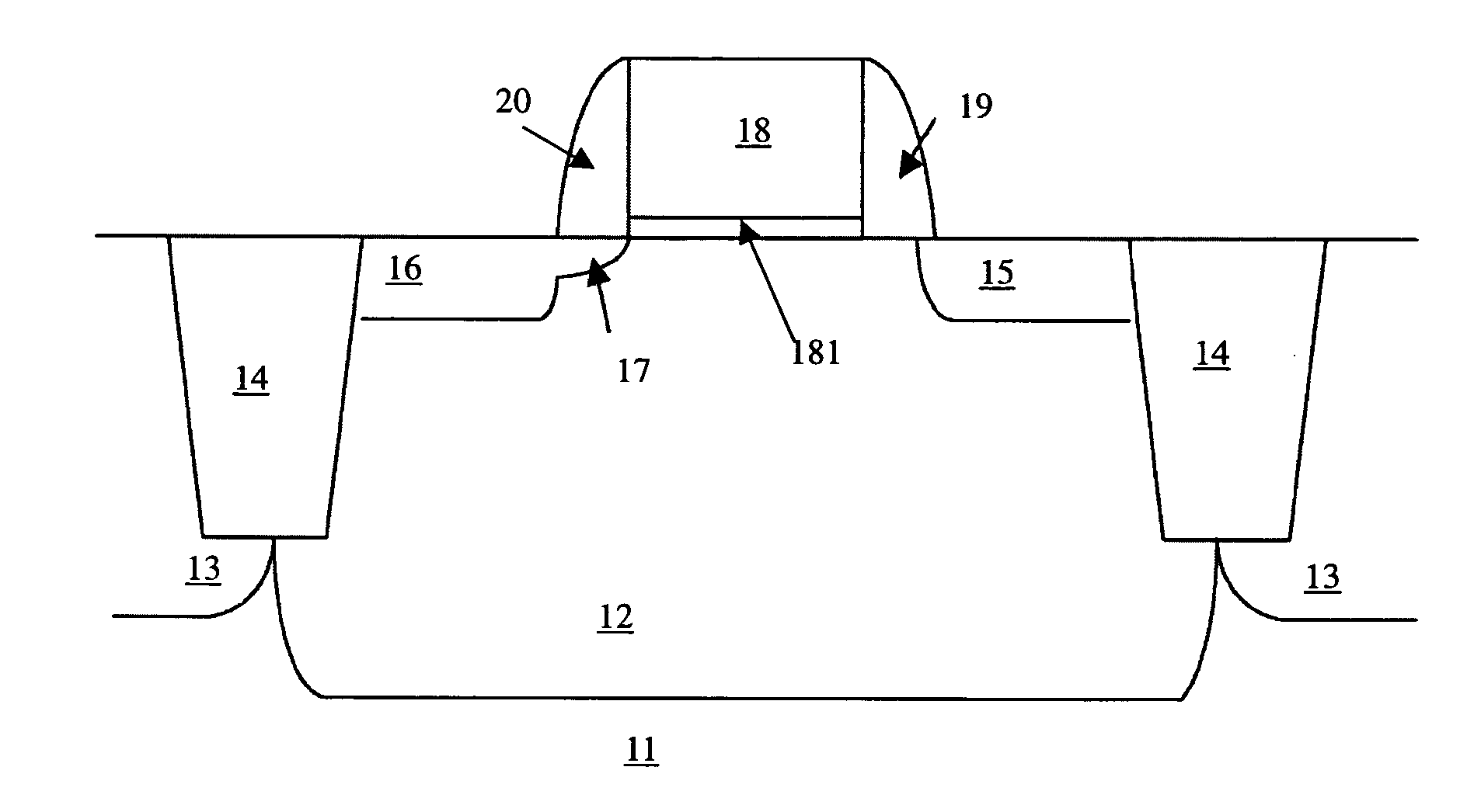
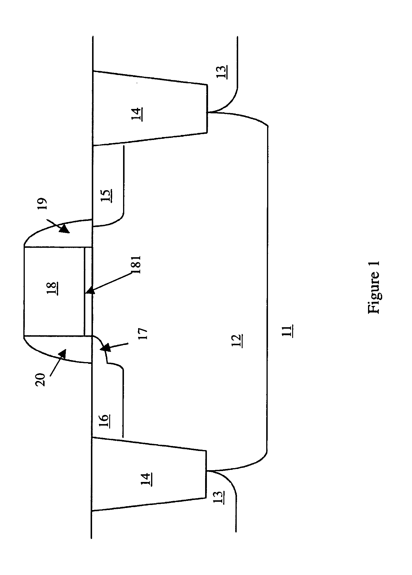
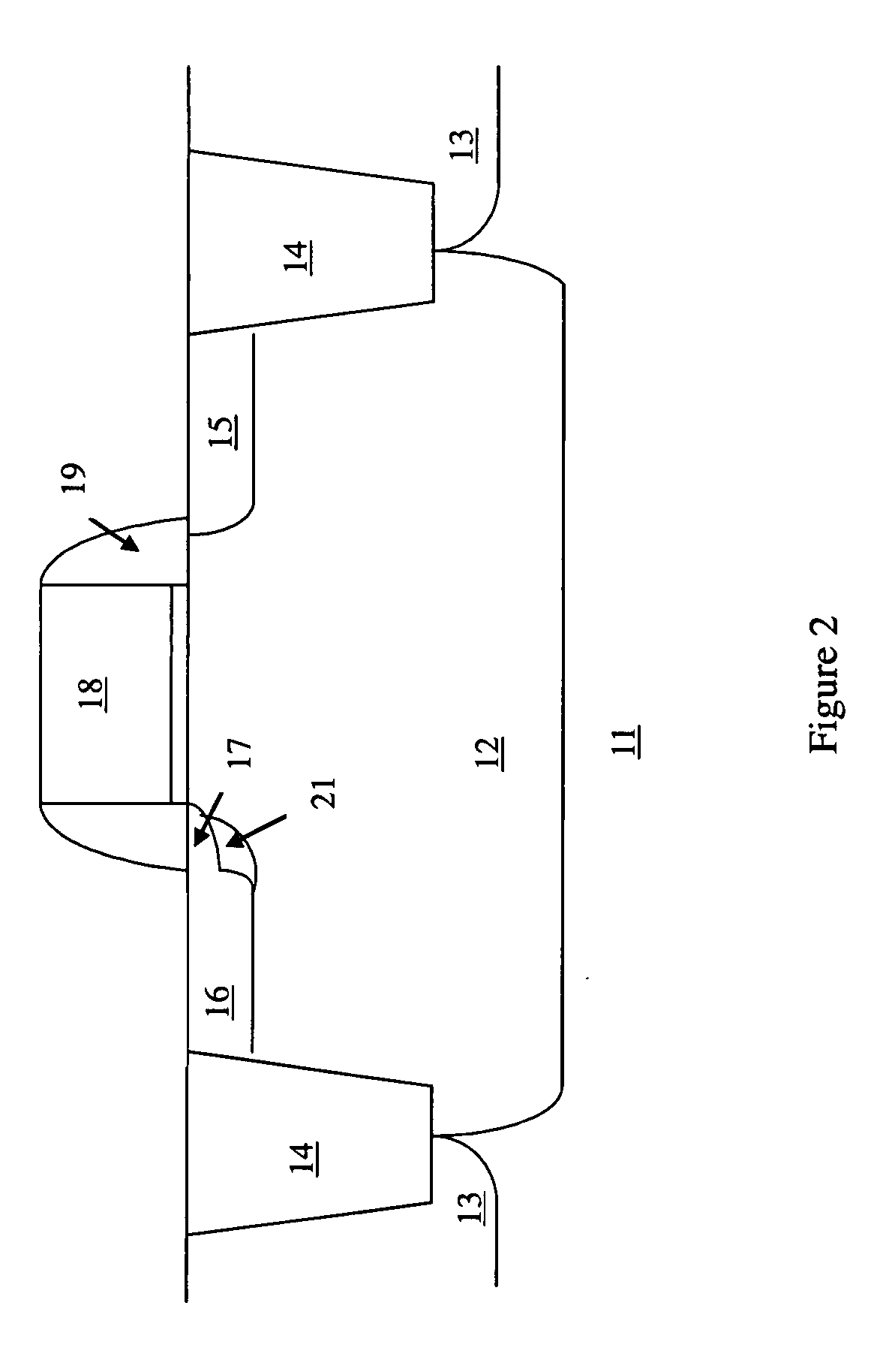
[0022]FIG. 1 shows a sectional view of an asymmetric-LDD MOS device according to the present invention. There are a P-substacte 11, a Pwell 12, a Nwell 13, a STI 14, a N+ drain electrode 15, a N+ source electrode 16, a N− LDD region 17, a gate electrode 18, a first spacer 20, and a second spacer 19 in FIG. 1. The P-substacte 11 and the Pwell 12 form a silicon substrate. The gate electrode 18 includes a gate insulating film adjacent to the Pwell 12. The first spacer 20 is adjacent to the N− LDD region 17, but the second spacer 19 is adjacent to the Pwell 12, which is the major difference to conventional MOS transistor. In other words, the major difference to the prior MOS transistor is no N− LDD region at drain side. Therefore, the formed depletion region under reverse drain bias can sustain large voltage for RF Power application.

[0023]According the present invention, the MOS device structure with spacer at both source and drain sides but only LDD implant at the source side. For a NM...


PUM


Abstract

The present invention proposes a new asymmetric-lightly-doped drain (LDD) metal oxide semiconductor (MOS) transistor that is fully embedded in a CMOS logic. The radio frequency (RF) power performance of both conventional and asymmetric MOS transistor is measured and compared. The output power can be improved by 38% at peak power-added efficiency (PAE). The PAE is also improved by 16% at 10-dBm output power and 2.4 GHz. These significant improvements of RF power performance by this new MOS transistor make the RF-CMOS system-on-chip design a step further. Index Terms—Lightly-doped-drain (LDD), metal oxide semiconductor field effect transistor (MOSFET), metal oxide semiconductor (MOS) transistor, radio frequency (RF) power transistor.

Description

FIELD OF THE INVENTION[0001]The present invention is related to an MOS device, particularly to an asymmetric-LDD MOS transistor device.BACKGROUND OF THE INVENTIONI. Introduction[0002]The rapid technology evolution of Si metal oxide semiconductor field effect transistor (MOSFET) is beneficial for integrated circuit (IC) design with higher device speed and cost reduction. Besides the advantages on digital performance, the scaling of CMOS technology also has largely improved the radio frequency (RF) performance of MOS devices. The most significant improvement along with CMOS technology scaling is the larger RF gain, higher cut-off frequency, and maximum oscillation frequency. This has made CMOS device technology the prime choice for RF system-on chip (SoC) application such as WCDMA, W-LAN, and ultra wide band (UWB) wireless communication. However, the low drain breakdown voltage of CMOS transistors restricts the use of CMOS for power amplifiers. This limitation for high voltage operati...

Claims


Application Information

Patent Timeline
IPC IPC(8): H01L29/78H01L29/76H01L29/94H01L31/00
CPCH01L29/1045H01L29/1083H01L29/7835H01L29/66659H01L29/66537
Inventor KING, MINGCHUCHIN, ALBERT
Owner KING MINGCHU
Why Eureka
Try Eureka