Manufacturing method for semiconductor chips

a manufacturing method and semiconductor technology, applied in the direction of semiconductor devices, basic electric elements, electrical equipment, etc., can solve the problems of increasing the difficulty of plasma ions reaching the etching bottom portion, reducing the transverse rupture strength of the semiconductor chip, and increasing the cost of the whole plasma dicing processing. , the effect of low cost efficiency

Active Publication Date: 2009-04-09
PANASONIC CORP
View PDF5 Cites 13 Cited by
  • Summary
  • Abstract
  • Description
  • Claims
  • Application Information

AI Technical Summary

Benefits of technology

[0068]Furthermore, by employing an insulating protective sheet as a protective sheet adhesively placed to protect the first surface of the semiconductor wafer, removing the portions that correspond to the dividing regions for the exposure of the insulating protective sheet and thereafter continuing the plasma etching in a state in which the exposed insulating protective sheet is electrically charged, the corner portions of the semiconductor chips can be removed, meaning that an effect similar to the aforementioned effect can be obtained.
[0069]Moreover, the plasma etching process is carried out without placing a mask layer on the second surface of the semiconductor wafer, and therefore, labor for carrying out the mask formation process and the removal process can be saved. In particular, the mask layer formation process necessary for the conventional semiconductor wafer dividing method has a high processing cost and is required to have complicated processing. Therefore, by making such a process unnecessary, a low-cost efficient semiconductor chip manufacturing method can be provided.
[0070]Moreover, by forming the dividing-groove portions formed on the second surface of the semiconductor wafer so that its depth dimension is not smaller than the thickness dimension of the semiconductor devices that are finally separated into individual pieces, the dividing-groove portions can be removed while allowing the thickness dimension of the semiconductor devices to be obtained by performing the plasma etching, and the separation into the semiconductor devices by the plasma etching accompanied by no mask layer formation (i.e., maskless) can concretely be achieved.
[0071]Moreover, a damaged layer is to be formed by the remaining stress and the like in the neighborhood of the surface of the dividing-groove portions in forming the dividing-groove portions. However, by performing the plasma etching also on the surfaces of the dividing-groove portions and finally removing the dividing-groove portions themselves, the removal of the formed damaged layer can be performed concurrently with the dividing process. Therefore, an efficient semiconductor chip manufacturing method that needs no special processing to be performed for the removal of the damaged layer can be achieved.
[0072]Moreover, when an abrading process for reducing the thickness of the semiconductor wafer is carried out on the second surface of the semiconductor wafer, a damaged layer is to be formed in the neighborhood of the second surface due to the abrading process. However, by performing the plasma etching on the entire second surface, removal of the damaged layer can be performed concurrently with the dividing process. Therefore, an efficient semiconductor chip manufacturing method that has no need to provide a process only for removing the damaged layer subsequent to the abrading process and is able to carry out the process concurrently with the plasma etching can be achieved.
[0073]Moreover, by forming the dividing-groove portions by means of a dicer that is the device used for the conventional mechanical dividing method, the cost of the total processes can be suppressed.

Problems solved by technology

In particular, the conventional plasma dicing described above has a characteristic that the ions in the plasma have increasing difficulties in reaching the etching bottom portion as getting closer to the bottom portion.
In such a case, there is a problem that the corner portions 554 become more easily chipped and the transverse rupture strength of the semiconductor chip is reduced.
Moreover, the mask used in the conventional plasma dicing as described above is generally formed by an optical method using photolithograph, and the mask formation by the photolithograph has the problem that the cost of the whole plasma dicing processing is increased by the addition of a complicated processing of high processing cost, and the processing cannot efficiently be achieved.

Method used


Image

  • Manufacturing method for semiconductor chips
  • Manufacturing method for semiconductor chips
  • Manufacturing method for semiconductor chips

Examples


first embodiment

Construction of Plasma Processing Apparatus

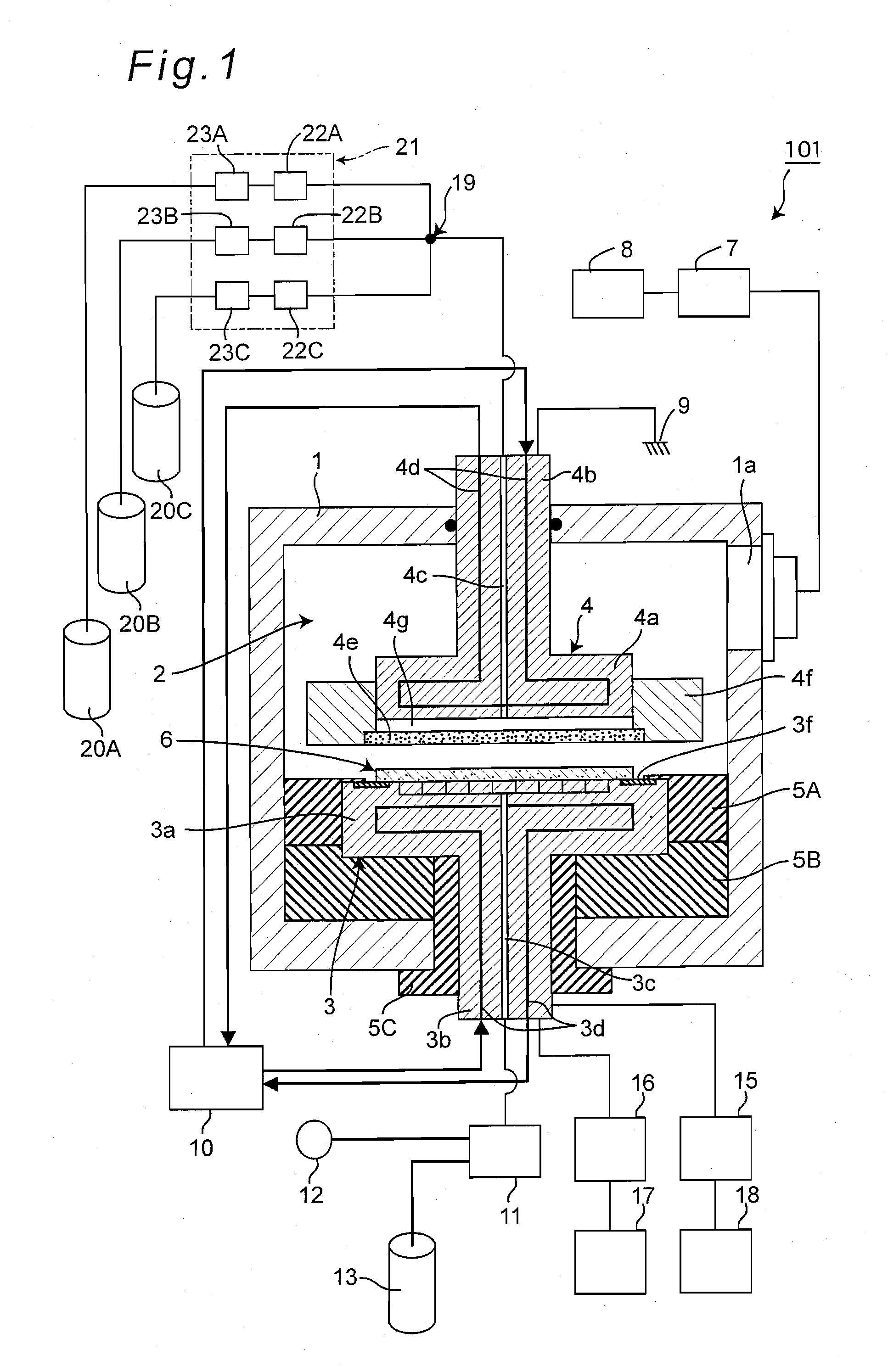
[0136]FIG. 1 shows a schematic structural view that schematically shows the construction of a plasma processing apparatus 101 used for dividing a semiconductor wafer by a manufacturing method for semiconductor chips of the first embodiment of the present invention. It is noted that FIG. 1 is a schematic structural view showing a longitudinal sectional view of the plasma processing apparatus 101. The plasma processing apparatus 101 is the apparatus that manufactures semiconductor chips by dividing a semiconductor wafer, on the circuit-formation-face (first surface) of which a plurality of semiconductor devices are formed, into individual pieces of the semiconductor chips that include the semiconductor devices.

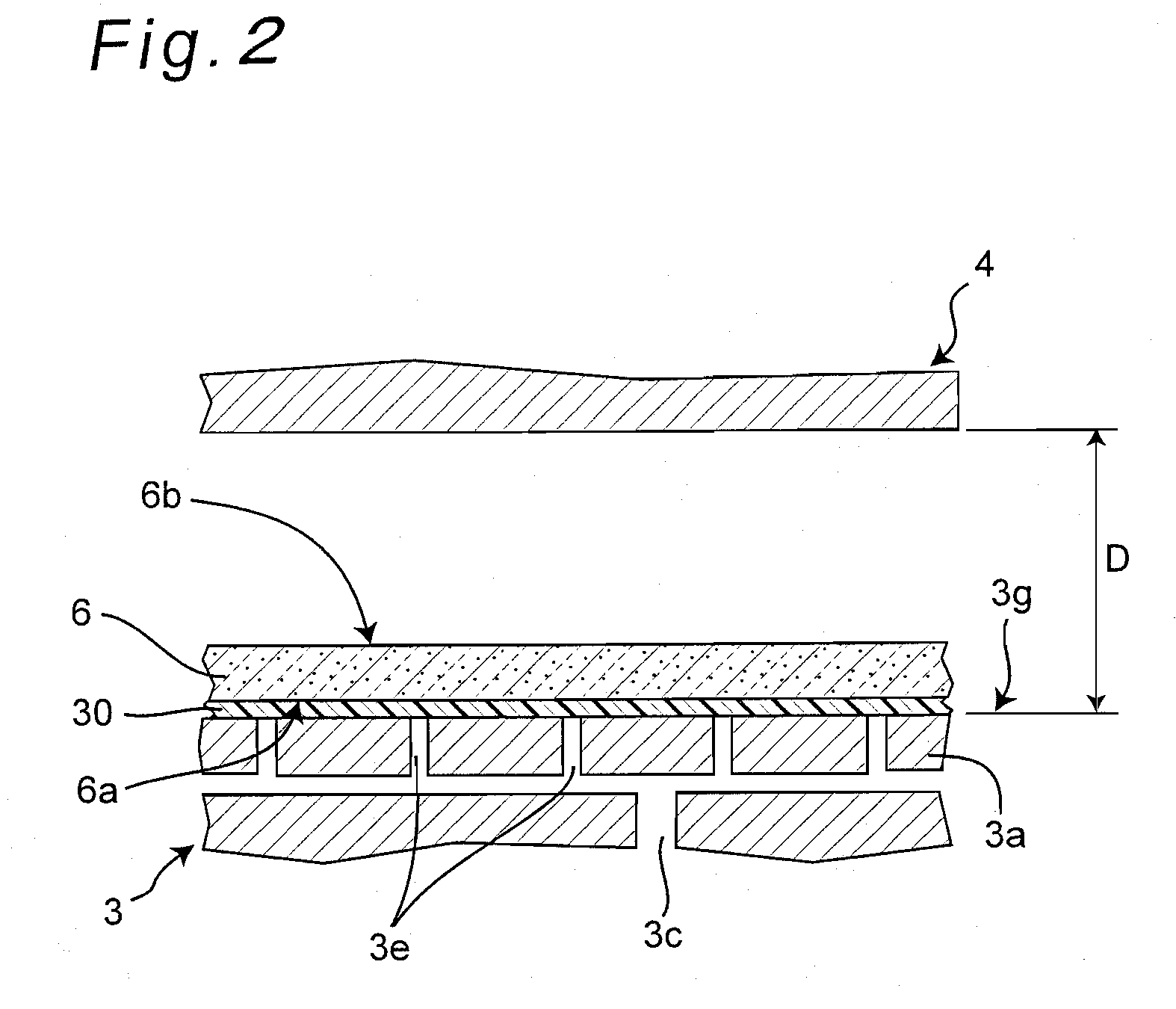
[0137]Moreover, in a series of semiconductor chip manufacturing processes as described above, a protective sheet made of, for example, a material that is less plasma etchable than silicon that is the principal material of the semiconduc...

second embodiment

[0228]The present invention is not limited to the above embodiment but allowed to be put into practice in various modes. For example, a manufacturing method for semiconductor chips according to the second embodiment of the present invention is described below with reference to the schematic explanatory views shown in FIG. 18, FIGS. 19A and 19B, FIGS. 20A and 20B and FIGS. 21A and 21B.

[0229]The manufacturing method for semiconductor chips of the present second embodiment differs from the first embodiment in the point that a polyimide (PI) film is used as the insulating film instead of using the silicon oxide film 35 as the insulating film formed in the portions that correspond to the dividing regions R2 as in the semiconductor wafer 6 of the first embodiment. Only the different point is described below. The fact that the plasma processing apparatus 101 used in the first embodiment is similarly used by the manufacturing method for semiconductor chips of the present second embodiment i...

modification example of second embodiment

[0239]Although the case where the polyimide film 146 formed as the surface protection film is used as the insulating film placed in the dividing regions R2 has been described above, the present second embodiment is not limited only to the case. It may be a case where, for example, a silicon nitride film formed of silicon nitride (Si3N4) is used as the surface protection film in place of such a case. The case where the silicon nitride film is used is described below as a semiconductor chip manufacturing method according to a modification example of the present second embodiment. Moreover, for the description, a flow chart showing the procedure of the semiconductor chip manufacturing method is shown in FIG. 22, and a schematic explanatory view showing a state in which a notch formation process and a silicon-nitride film (insulator) removal process are concurrently carried out is shown in FIG. 23.

[0240]First of all, as shown in the flow chart of FIG. 22, the loading of a semiconductor ...


PUM


Abstract

By forming dividing-groove portions in accordance with dividing regions on the second surface of a semiconductor wafer where an insulating film is placed in the dividing regions of the first surface and performing etching of the entire second surface and the surfaces of the dividing-groove portions by performing plasma etching from the second surface, corner portions on the second surface side are removed, while the insulating film is exposed from the etching bottom portion by removing the dividing-groove portions in the dividing regions. And by continuously performing the plasma etching in a state in which the exposed insulating film is surface charged with electric charge due to ions in plasma, corner portions on the first surface side put in contact with the insulating film are removed, and semiconductor chips that have a high transverse rupture strength are provided.

Description

TECHNICAL FIELD[0001]The present invention relates to a manufacturing method for semiconductor chips for forming semiconductor devices arranged in a plurality of device-formation-regions defined by dividing regions on a first surface of a semiconductor wafer and individually separating the device-formation-regions of the semiconductor wafer along the dividing regions, thereby manufacturing semiconductor chips that include the individualized semiconductor devices and to a semiconductor chip.BACKGROUND ART[0002]Conventionally, as a method for dividing a semiconductor wafer into individual semiconductor chips by such a manufacturing method for semiconductor chips, various methods have been known. For example, a method for dividing a semiconductor wafer by mechanically cutting the wafer by means of a rotary blade called the dicer blade, i.e., mechanical dicing is known.[0003]However, semiconductor wafers have recently been made thinner and thinner, and a semiconductor wafer susceptible ...

Claims


Application Information

Patent Timeline
Patent Type & Authority Applications(United States)
IPC IPC(8): H01L21/302
CPCH01L21/3065H01L21/6835H01L21/78H01L2924/30105H01L2221/6834H01L2221/68354H01L2924/10158H01L29/0657
Inventor ARITA, KIYOSHINAKAGAWA, AKIRA
Owner PANASONIC CORP
Why Eureka
Try Eureka